

Semiconductor packaging
Semiconductor packaging is a crucial component of modern electronics fabrication since it protects and connects integrated circuits to the outside world. IC packaging has developed to satisfy the demands of many applications as electronic devices have grown smaller, quicker, and more adaptable. This article discusses the various kinds of semiconductor packaging, and their significance, used for manufacturing in the semiconductor industry.
Types of Semiconductor Packaging
Semiconductor packaging entails enclosing the semiconductor die within a protective package may be made of ceramic or plastic and connecting the device electrically. The packaging type chosen is determined by criteria such as form factor, thermal concerns, electrical performance, and cost. Here are some examples of several different types of IC packaging:
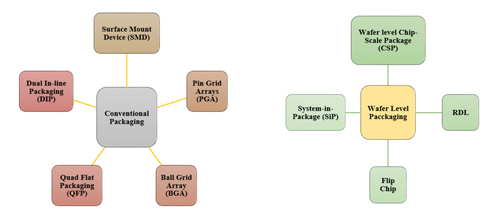
- Dual In-line Package (DIP): DIP is one of the oldest semiconductor packaging types, and it remains popular in the industry. It is inserted through the hole-type package in the circuit board. Its pin counts range from 8 to 64.
- Quad Flat Package (QFP): QFP is a surface-mount package that is rectangular in shape and has leads protruding from all four sides. QFP packages are offered in pin counts ranging from 32 to 304.
- Small Outline J-lead Package (SOJ): SOJ is a surface-mount package that features J-shaped leads on both sides. SOJ packages are available with pin counts ranging from 8 to 44.
- Pin Grid Array (PGA): PGA is a through-hole package with pins positioned on the bottom of the package in a grid arrangement. PGA packages come in a variety of pin counts, ranging from 84 to 1,520.
- Ball Grid Array (BGA): BGA is surface-mount type packaging in which pins in the earlier packaging are replaced with a variety of solder balls. BGA packets come in a variety of ball counts, ranging from 4 to 2,500.
- Wafer-Level Packaging (WLP): WLP is a packaging method that involves encapsulating the ICs at the wafer level before being divided into individual chips. WLP packages come in a variety of sizes, ranging from 1 mm to 10 mm. Examples include RDL-based, flip-chip, and TSV-based packages. There are main two types of Wafer-level Chip-Scale Packages (WLCSP) that are Fan-In WLCSP and Fan-out WLCSP. Wherein the word “Fan” refers to the chip’s size.
- Fan-In WLCSP: The Fan-In WLCSP includes the insulating layer, solder balls right on top of the wafer, and package wiring all contributing to the different benefits of a fan-in WLCSP. It has an interposer that is the same size as the die. The electrical transmission channel is relatively short since the solder balls are connected to the chip directly rather than through a medium like a substrate, which enhances electrical properties.
- Fan-out WLCSP: Fan-out WLCSP overcomes the drawbacks of fan-in WLCSP while retaining its benefits. Fan-out WLCSP has package-mounted solder balls that can be “fanned out” away from the chip. The interposer’s size is the same as that of the die. It also offers good electrical characteristics like FI-WLCSP.
Importance of IC packaging:
- Electrical Performance: The packaging has an impact on the device’s electrical properties, and well-designed packaging reduces signal deterioration and improves overall performance.
- Thermal Control: Modern ICs produce a lot of heat. Heat dissipation is facilitated by efficient packaging designs, which helps avoid overheating and ensures long-term dependability.
- Form Factor & Size: As electronics get smaller and more portable, miniature packaging techniques make it possible to make devices that are svelte and tiny.
- Protection: Different packaging types protect the IC from various conditions including moisture, dust, and temperature changes. The packaging acts as a shield to protect the semiconductor die from these factors.
- Interconnect Density: The number of interconnects that may be accommodated depends on the kind of packaging. Complex interconnections are made possible by high-density packing, such as BGAs and CSPs, which is essential for contemporary electronics.
Techinsights images of Wafer level chip scale-type packaging
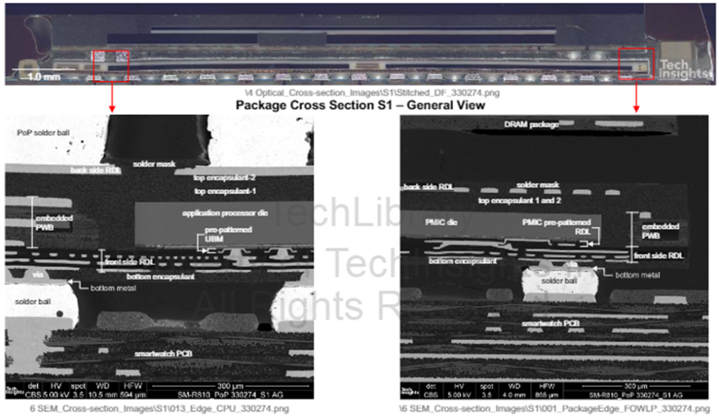
Figure 1 Samsung Exynos 9110 Processor (Source)
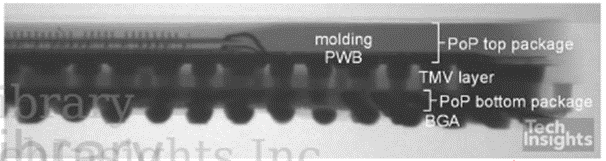
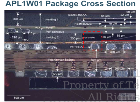
Figure 2 Apple A14 Bionic Processor (APL1W01) (Source)
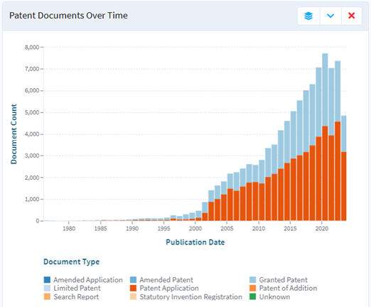
IP Trends in Wafer-Level Chip Scale Packaging in Semiconductor
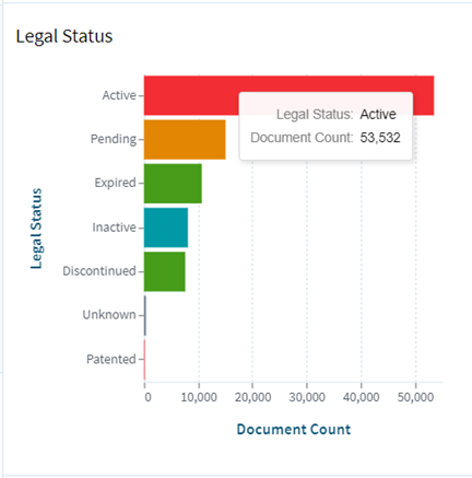
As the importance of packaging is increasing, there is a rapid growth in the patent filing trends witnessed across the globe. The Highest number of patents granted was in 2020 with 3339 patents and the highest number of patent applications filed was ~4553 in 2022.
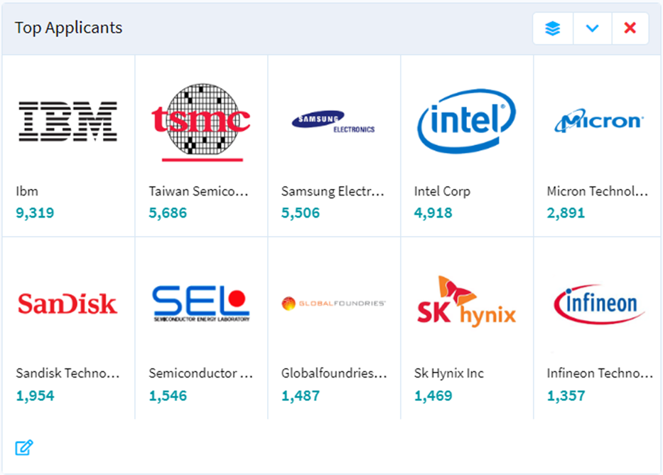
IBM is a dominant player in the market with ~9319 patent families. So far, it has 1.5 times more patent families than TSMC, which comes second with 5686 patent families. Samsung is the third-largest patent holder in the domain.
Other key players who have filed for patents in WLCSP technology are Intel, Micron, Globalfoundries, SanDisk, Infineon Technology, SK Hynix and so more.
(Source: Lens.org)
(Source: Lens.org)
Conclusion
IC packaging is a crucial step in the semiconductor business because it shields semiconductor components from corrosion and physical harm from the outside world. The many distinct varieties of IC packages are based on various circuit designs and requirements for the outside shell. The most popular IC packaging designs are wafer-level packaging, pin grid arrays, dual in-line packages, quad flat packages, compact outline J-lead packages, and chip carriers. The IC package you choose depends on the particular application requirements.