High Bandwidth Memory (HBM3)
JEDEC has released HBM3 with the JESD238A standard. It offers multiple advantages over previous releases of HBM technology in terms of speed, latency, and computational capabilities. The HBM3 technology implements RAS architecture for reducing memory error rates.
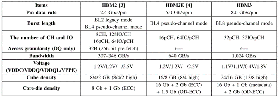
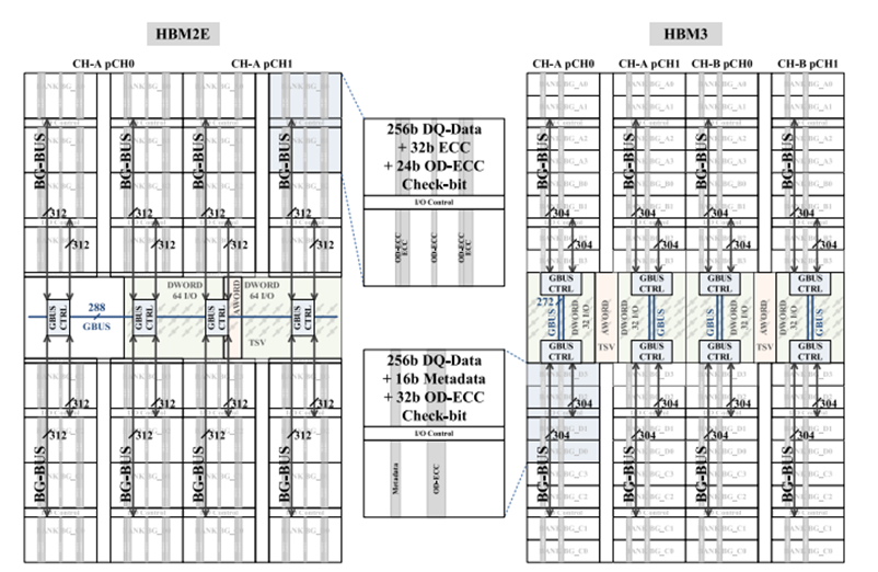
Second Generation of HBM implements 2.4 Gb/s/pin with 307-346 GB/s. Further, HBM2E implements 5.0 Gb/s/pin with 640 Gb/s, and third Generation of HBM implements 8.0 Gb/s/pin with 1024 GB/s.
A table describing about comparison of HBM2, HBM2E, And HBM3:
We have tried collecting all available information on the internet related to the HBM3 memory system. The blog includes documents of different versions of standards, related products, and IEEE Papers from manufacturers.
Different HBM standards released by JEDEC
Multiple version of the HBM memory system and their links are:
HBM1: JESD235: (Oct 2013): https://www.jedec.org/sites/default/files/docs/JESD235.pdf
HBM2: JESD235A: (Nov 2015): https://web.archive.org/web/20220514151205/https://composter.com.ua/documents/JESD235A.pdf
HBM2E: JESD235B: (Nov 2018): not available
HBM2 Update: JESD235C: (Jan 2020): not available
HBM1, HBM2: JESD235D: : (Feb 2021): https://www.jedec.org/sites/default/files/docs/JESD235D.pdf
HBM3: JESD238: (Jan 2022): not available
HBM3 update: JESD238A: (Jan 2023): https://www.jedec.org/sites/default/files/docs/JESD238A.pdf
HBM1:
JEDEC released the first version of the HBM standard, named HBM1 (JESD235 standard), in October 2013, and its link is below:
https://www.jedec.org/sites/default/files/docs/JESD235.pdf
HBM2:
JEDEC released the second version of the HBM standard, named HBM2 (JESD235A standard), in November 2015, and its link is below:
https://web.archive.org/web/20220514151205/https://composter.com.ua/documents/JESD235A.pdf
Further, JEDEC released the third version of the HBM standard named HBM2E (JESD235B standard) in November 2018 and HBM2 Updation (JESD235C) in January 2020. The link is not available on the internet.
HBM3:
JEDEC released a new version of the HBM standard named HBM3 (JESD238A standard) on Jan 2023, and its link is
https://www.jedec.org/sites/default/files/docs/JESD238A.pdf
Multiple new Features introduced in HBM3 are:
New features introduced in HBM3 for increasing memory speed and reducing memory latency are:
- On-Die DRAM ECC Operation
- Automated on-die error scrubbing mechanism (Error Check and Scrub (ECS) operation)
- MBIST enhanced memory built-in self-test (MBIST)
- WDQS Interval Oscillator
- Duty Cycle Adjuster (DCA) | Duty Cycle Monitor (DCM)
- Self-Repair Mechanism
Different IEEE Papers from other manufacturers are available. Manufacturers are working on HBM3 memory standard JEDEC JESD238A for various memory operations. They are implementing a new mechanism introduced in the HBM3 standard.
Samsung and SK Hynix are significant manufacturers of HBM3 and have revealed many research papers stating or indicating their implementation of different features of HBM3. The paper describes how various implemented technical features are introduced in the HBM3 memory system.
Products implementing HBM3 technology:

SAMSUNG HBM3 ICEBOLT:
The memory system stacks 12 stacks of DRAM memory systems for AI operations. It provides processing speeds up to 6.4Gbps and bandwidth that reaches 819GB/s.
Link to this product: https://semiconductor.samsung.com/dram/hbm/hbm3-icebolt/
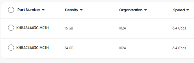
SKHYNIX HBM3 memory system:
SKhynix announces 12 layers of HBM3 with 24 GB memory capacity
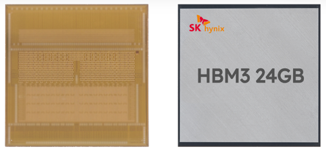
Link to this product: https://news.skhynix.com/sk-hynix-develops-industrys-first-12-layer-hbm3/
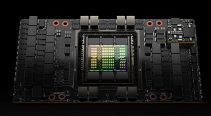
Nvidia Hopper H100 GPU implementing HBM3 memory system:
IEEE Papers from different Manufacturers exploring HBM3 technology
IEEE papers and their links from Samsung, SK Hynix, and Nvidia are mentioned. These papers are written authors from Samsung, SK Hynix, and Nvidia. The authors are exploring different technological aspects of the HBM3 memory system. The IEEE paper shows the architecture of the HBM memory system and various features:
Samsung IEEE paper related to HBM3:
Samsung has been working on HBM3 technology and has already released multiple products about it.
IEEE Paper1:
Title: A 4nm 1.15TB/s HBM3 Interface with Resistor-Tuned Offset-Calibration and In-Situ Margin-Detection
DOI: 10.1109/ISSCC42615.2023.10067736
Link: https://ieeexplore.ieee.org/document/10067736
IEEE Paper2:
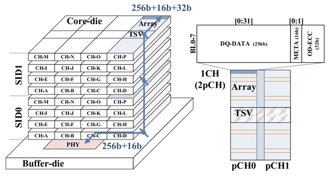
Title: A 16 GB 1024 GB/s HBM3 DRAM with On-Die Error Control Scheme for Enhanced RAS Features
DOI: 10.1109/VLSITechnologyandCir46769.2022.9830391
Link: https://ieeexplore.ieee.org/document/9830391
IEEE Paper3:
Title: A 16 GB 1024 GB/s HBM3 DRAM With Source-Synchronized Bus Design and On-Die Error Control Scheme for Enhanced RAS Features
DOI: 10.1109/JSSC.2022.3232096
Link: https://ieeexplore.ieee.org/document/10005600
SK Hynix IEEE paper related to HBM3:
SK Hynix has also published 2 IEEE papers describing the HBM3 memory technological aspect.
IEEE Paper 1 and IEEE Paper 2 of SK Hynix:
IEEE Paper1:
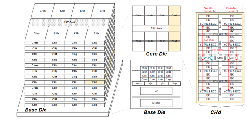
Title: A 192-Gb 12-High 896-GB/s HBM3 DRAM With a TSV Auto-Calibration Scheme and Machine-Learning-Based Layout Optimization|
DOI: 10.1109/ISSCC42614.2022.9731562
Link: https://ieeexplore.ieee.org/document/9731562
IEEE Paper2:
Title: A 192-Gb 12-High 896-GB/s HBM3 DRAM With a TSV Auto-Calibration Scheme and Machine-Learning-Based Layout Optimization
DOI: 10.23919/VLSIC.2019.8778082
Link: https://ieeexplore.ieee.org/document/8778082/
Nvidia IEEE paper related to HBM3:
Nvidia has also published 1 IEEE paper about the HBM3 memory system. The paper describes that Hopper H100 GPU is implementing five HBM memory systems with a total memory bandwidth of over 3TB/s.
IEEE Paper1:
Title: NVIDIA Hopper H100 GPU: Scaling Performance
DOI: 10.1109/ISSCC42614.2022.9731562
Link: https://ieeexplore.ieee.org/abstract/document/10070122
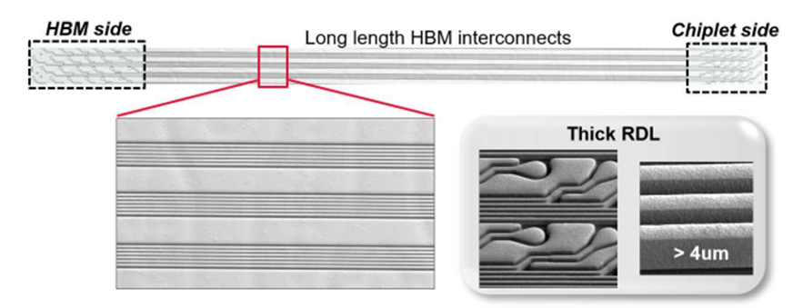
TSMC IEEE paper related to HBM3:
TSMC has also published 1 IEEE paper pertaining to the HBM3 memory system. The paper implements integrated de-cap capacitors for suppressing power domain noise and for enhancing the HBM3 signal integrity at a high data rate.
IEEE Paper1:
Title: Heterogeneous and Chiplet Integration Using Organic Interposer (CoWoS-R)
DOI: 10.1109/ISSCC42614.2022.9731562
Link: https://ieeexplore.ieee.org/document/10019517/