Categories
Electronics

YMTC X1-9050: A New Generation of 3D NAND Flash Memory

Yangtze Memory Technologies Co., Ltd (YMTC) has remained a leader in its field despite the rapid changes happening around it. Today, we will examine one of their notable products, the X1-9050.

YMTC X1-9050

What is the X1-9050?

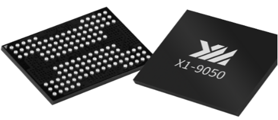
The X1-9050 is the second generation of YMTC’s 3D NAND flash memory products. An important turning point for the company was reached in August 2019 when it was placed into small-scale mass production. One distinctive feature that makes this product stand out in the market is that it is the first from YMTC to be designed and processed using the Xtacking architecture.

X1-9050 Layout

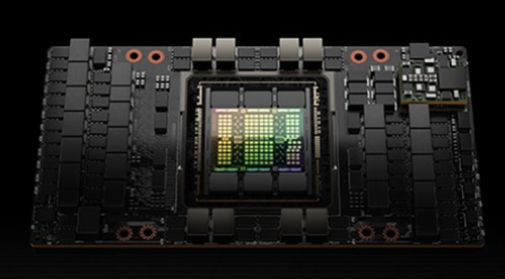
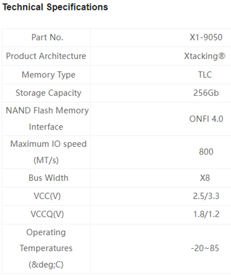
X1-9050 Layout (Source: https://www.ymtc.com/cn/technicalintroduction.html)

With its cutting-edge features and capabilities, the X1-9050 is a storage solution of the future. Its versatility in different settings is attributed to its distinctive characteristics. The X1-9050 can meet your needs whether you’re a professional handling massive volumes of data, a student needing dependable storage for assignments, or a gamer needing fast performance.

X1-9050 Key Features

Advanced Technology

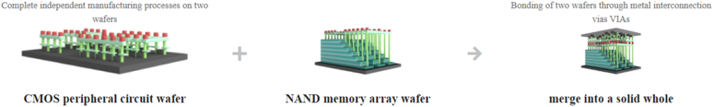
The X1-9050 is a product of advanced technology. It’s built on the Xtacking architecture, which is YMTC’s patented 3D NAND stacking technology. The peripheral and memory cell arrays can now be manufactured independently thanks to this technology, which can greatly increase chip production efficiency.

Increased Speed

The X1-9050 comes with a 256 GB chip capacity, which makes it an excellent choice for those seeking large quantities of storage. It also offers an impressive I/O speed of upto800MT/s.

Future of Storage

The X1-9050 is a revolutionary storage solution that offers advanced technology and impressive features. As data generation continues to rise, it represents the future of digital storage. Supported by mainstream industry controllers, it can be widely used in the development of consumer, enterprise, and mobile storage products, showcasing the future of digital storage.

Other key differentiating features in X1-9050

The X1-9050 stands out for several reasons when selecting a 3D NAND flash memory product. Its blend of high capacity and speed is unquestionably a significant selling point. Yet, past that, the utilization of the Xtacking design offers extra advantages, adding to the item’s general presentation and unwavering quality.

YMTC X1-9050 v/s Acer Predator GM7

The X1-9050 uses the Xtacking architecture. This unique architecture allows for independent manufacturing of the peripheral and memory cell arrays, which can significantly enhance the efficiency of the chip production process. This is a feature that sets the X1-9050 apart from many of its competitors, including the Acer Predator GM7.

YMTC X1-9050 - Technical Specifications
Acer Predator GM7 - Technical Specifications

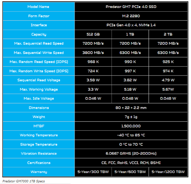
YMTC X1-9050 v/s Acer Predator GM7: Specs comparison (Source: https://www.ymtc.com/en/products/4.html?cat=35 and https://www.servethehome.com/predator-gm7-1tb-pcie-gen4-nvme-ssd-review/)

The X1-9050 likewise offers noteworthy speed. With a chip limit of 256GB, the X1-9050 offers significant extra room. This high capacity makes it a strong decision for those needing huge capacity. While the Acer Hunter GM7 likewise offers significant capacity, the X1-9050’s ability is explicitly intended for 3D NAND flash memory, making it a more particular decision. With a greatest I/O speed that can reach up to 800MT/s, it likewise beats numerous rivals in its class.

Patent Landscape

The Yangtze Memory Technologies Co., Ltd. (YMTC) X1-9050, a 2nd-generation 3D NAND flash memory product, has been making waves in the memory industry. The technology landscape surrounding this product is rich and diverse, with a significant increase in patent filings globally. The growth in patent filings for this technology has been remarkable. YMTC has made significant investments in research and development since its inception and has filed more than 4000 memory-related patents. In the years 2020 and beyond, the number of patent application filings increased by 3.97 percent. This development means fast headways in 3D NAND innovation and the rising interest of organizations in this space.

YMTC patent applications per year

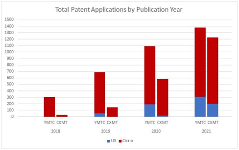
YMTC patent applications per year (Source: https://www.semiconductor-digest.com/china-semiconductor-firms-aggressively-filing-patents-as-they-expand-operations/)

The organization behind the arrival of X1-9050, YMTC is viewed as the pillar behind all the 3D NAND innovations. YMTC has successfully developed 3D NAND SSD products with even higher density by combining their own process and design technology based on Xtacking hybrid bonding. The all-new 232L Xtacking 3.0 TLC is a foundational one and may also guide the development of similar technologies shortly. The Yangtze Memory Technologies Co., Ltd. (YMTC) X1-9050, a 2nd-generation 3D NAND flash memory product, has been making waves in the memory industry.

YMTC 3D NAND bit Density Trend

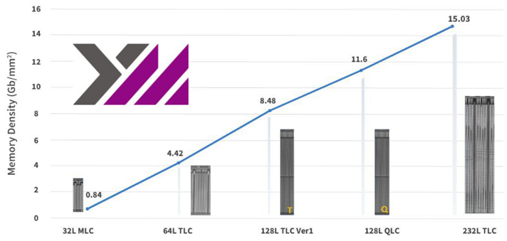
YMTC 3D NAND bit density trend (Source: https://www.techinsights.com/blog/ymtc-leading-pioneer-3d-nand)

Several companies are actively filing patents in this area. YMTC, the creator of the X1-9050, is at the forefront. It has been frequently filing patents and obtaining most of its patent rights in less than 500 days. This could be due to strong innovation or China’s patent policy. In addition to YMTC, other companies like Micron Technology have also been involved in the patent landscape.

Key manufacturers of 3D NAND

Key manufacturers of 3D NAND (Source: https://www.storagenewsletter.com/2020/11/06/3d-nand-market-to-grow-to-81-billion-in-2025/)

Conclusion

In the rapidly advancing tech industry, the X1-9050 is a testament to YMTC’s commitment to innovation and quality. Whether you’re a consumer looking for reliable storage solutions, or a business seeking to enhance your tech offerings, the X1-9050 is a product worth considering.

Categories
Computer Science

High Bandwidth Memory (HBM3) Products | SK Hynix | Samsung | Nvidia and related IEEE Papers

High Bandwidth Memory (HBM3)

JEDEC has released HBM3 with the JESD238A standard. It offers multiple advantages over previous releases of HBM technology in terms of speed, latency, and computational capabilities. The HBM3 technology implements RAS architecture for reducing memory error rates.

Second Generation of HBM implements 2.4 Gb/s/pin with 307-346 GB/s. Further, HBM2E implements 5.0 Gb/s/pin with 640 Gb/s, and third Generation of HBM implements 8.0 Gb/s/pin with 1024 GB/s.

A table describing about comparison of HBM2, HBM2E, And HBM3:

We have tried collecting all available information on the internet related to the HBM3 memory system. The blog includes documents of different versions of standards, related products, and IEEE Papers from manufacturers.

Different HBM standards released by JEDEC

Multiple version of the HBM memory system and their links are:

HBM1: JESD235: (Oct 2013): https://www.jedec.org/sites/default/files/docs/JESD235.pdf 
HBM2: JESD235A: (Nov 2015): https://web.archive.org/web/20220514151205/https://composter.com.ua/documents/JESD235A.pdf
HBM2E: JESD235B: (Nov 2018): not available
HBM2 Update: JESD235C: (Jan 2020): not available
HBM1, HBM2: JESD235D: : (Feb 2021): https://www.jedec.org/sites/default/files/docs/JESD235D.pdf
HBM3: JESD238: (Jan 2022): not available
HBM3 update: JESD238A: (Jan 2023): https://www.jedec.org/sites/default/files/docs/JESD238A.pdf

HBM1: 

JEDEC released the first version of the HBM standard, named HBM1 (JESD235 standard), in October 2013, and its link is below:

https://www.jedec.org/sites/default/files/docs/JESD235.pdf

HBM2:

JEDEC released the second version of the HBM standard, named HBM2 (JESD235A standard), in November 2015, and its link is below:

https://web.archive.org/web/20220514151205/https://composter.com.ua/documents/JESD235A.pdf

Further, JEDEC released the third version of the HBM standard named HBM2E (JESD235B standard) in November 2018 and HBM2 Updation (JESD235C) in January 2020. The link is not available on the internet.

HBM3:

JEDEC released a new version of the HBM standard named HBM3 (JESD238A standard) on Jan 2023, and its link is

https://www.jedec.org/sites/default/files/docs/JESD238A.pdf

Multiple new Features introduced in HBM3 are:

New features introduced in HBM3 for increasing memory speed and reducing memory latency are:

  1. On-Die DRAM ECC Operation
  2. Automated on-die error scrubbing mechanism (Error Check and Scrub (ECS) operation)
  3. MBIST enhanced memory built-in self-test (MBIST)
  4. WDQS Interval Oscillator
  5. Duty Cycle Adjuster (DCA) | Duty Cycle Monitor (DCM)
  6. Self-Repair Mechanism


Different IEEE Papers from other manufacturers are available. Manufacturers are working on HBM3 memory standard JEDEC JESD238A for various memory operations. They are implementing a new mechanism introduced in the HBM3 standard.

Samsung and SK Hynix are significant manufacturers of HBM3 and have revealed many research papers stating or indicating their implementation of different features of HBM3. The paper describes how various implemented technical features are introduced in the HBM3 memory system.

Products implementing HBM3 technology:

Products implementing HBM3 technology

SAMSUNG HBM3 ICEBOLT:

The memory system stacks 12 stacks of DRAM memory systems for AI operations. It provides processing speeds up to 6.4Gbps and bandwidth that reaches 819GB/s.

SAMSUNG HBM3 ICEBOLT
Fig 1. Samsung HBM3 ICEBOLT variants

Link to this product: https://semiconductor.samsung.com/dram/hbm/hbm3-icebolt/

SKHYNIX HBM3 memory system:

SKhynix announces 12 layers of HBM3 with 24 GB memory capacity

Fig 2. SK Hynix HBM3 24 GB memory system

Link to this product: https://news.skhynix.com/sk-hynix-develops-industrys-first-12-layer-hbm3/

Nvidia Hopper H100 GPU implementing HBM3 memory system:

Nvidia Hopper H100 GPU implementing HBM3 memory system
Fig 3. Nvidia Hopper H100 GPU implementing HBM3 memory system

IEEE Papers from different Manufacturers exploring HBM3 technology

IEEE papers and their links from Samsung, SK Hynix, and Nvidia are mentioned. These papers are written authors from Samsung, SK Hynix, and Nvidia. The authors are exploring different technological aspects of the HBM3 memory system. The IEEE paper shows the architecture of the HBM memory system and various features:

Samsung IEEE paper related to HBM3:

Samsung has been working on HBM3 technology and has already released multiple products about it.

IEEE Paper1:

Title: A 4nm 1.15TB/s HBM3 Interface with Resistor-Tuned Offset-Calibration and In-Situ Margin-Detection
DOI10.1109/ISSCC42615.2023.10067736
Link: https://ieeexplore.ieee.org/document/10067736

IEEE Paper2:

Title: A 16 GB 1024 GB/s HBM3 DRAM with On-Die Error Control Scheme for Enhanced RAS Features
DOI10.1109/VLSITechnologyandCir46769.2022.9830391
Link: https://ieeexplore.ieee.org/document/9830391

IEEE Paper3:

Title: A 16 GB 1024 GB/s HBM3 DRAM With Source-Synchronized Bus Design and On-Die Error Control Scheme for Enhanced RAS Features
DOI10.1109/JSSC.2022.3232096
Link: https://ieeexplore.ieee.org/document/10005600

Samsung HBM3 Architecture
Fig 4. Samsung HBM3 architecture

Data-bus architecture of HBM2E and HBM3
Fig 5. Data-bus architecture of HBM2E and HBM3

SK Hynix IEEE paper related to HBM3:

SK Hynix has also published 2 IEEE papers describing the HBM3 memory technological aspect.

IEEE Paper 1 and IEEE Paper 2 of SK Hynix:

IEEE Paper1:

Title: A 192-Gb 12-High 896-GB/s HBM3 DRAM With a TSV Auto-Calibration Scheme and Machine-Learning-Based Layout Optimization|
DOI: 10.1109/ISSCC42614.2022.9731562
Link: https://ieeexplore.ieee.org/document/9731562

IEEE Paper2:

Title: A 192-Gb 12-High 896-GB/s HBM3 DRAM With a TSV Auto-Calibration Scheme and Machine-Learning-Based Layout Optimization
DOI: 10.23919/VLSIC.2019.8778082
Link: https://ieeexplore.ieee.org/document/8778082/

SK Hynix architecture of HBM3 memory system
Fig 6. SK Hynix architecture of HBM3 memory system.

Nvidia IEEE paper related to HBM3:

Nvidia has also published 1 IEEE paper about the HBM3 memory system. The paper describes that Hopper H100 GPU is implementing five HBM memory systems with a total memory bandwidth of over 3TB/s.

IEEE Paper1:

Title: NVIDIA Hopper H100 GPU: Scaling Performance
DOI10.1109/ISSCC42614.2022.9731562
Link: https://ieeexplore.ieee.org/abstract/document/10070122

Nvidia Hopper H100 implementing HBM3 memory system
Fig 7. Nvidia Hopper H100 implementing HBM3 memory system.

TSMC IEEE paper related to HBM3:

TSMC has also published 1 IEEE paper pertaining to the HBM3 memory system. The paper implements integrated de-cap capacitors for suppressing power domain noise and for enhancing the HBM3 signal integrity at a high data rate.

IEEE Paper1:

Title: Heterogeneous and Chiplet Integration Using Organic Interposer (CoWoS-R)
DOI10.1109/ISSCC42614.2022.9731562
Link: https://ieeexplore.ieee.org/document/10019517/

HBM and Chiplet side of a system
Fig 8. HBM and Chiplet side of a system

Categories
Electronics Others

Migration from Hybrid Memory Cube (HMC) to High-Bandwidth Memory (HBM)

Introduction:

Memory technology plays a vital role in providing effective data processing as the demand for high-performance computing keeps rising. The industry has recently seen a considerable migration from Hybrid Memory Cube (HMC) to High-Bandwidth Memory (HBM) because of HMB’s higher performance, durability, and scalability. This technical note talks about the causes behind the widespread adoption of HBM as well as the benefits it has over HMC.

HBM Overview:

HBM is a revolutionary memory technology that outperforms conventional memory technologies. HBM is a vertically stacked DRAM memory device interconnected to each other using through-silicon vias (TSVs). HBM DRAM die is further tightly connected to the host device using its distribution channels which are completely independent of one another. This architecture is used to achieve high-speed, low-power operation. HBM has a reduced form factor because it combines DRAM dies and logic dies in a single package, making it ideal for space-constrained applications. An interposer that is interconnected to the memory stacks, enables high-speed data transmission between memory and processor units. 

HMC Brief:

The Hybrid Memory Cube (HMC) comprises multiple stacked DRAM dies and a logic die, stacked together using through-silicon via (TSV) technology in a single-package 3D-stacked memory device. The HMC stack’s memory dies each include their memory banks as well as a logic die for memory access control. It was developed by Micron Technology and Samsung Electronics Co. Ltd. in 2011, and announced by Micron in September 2011.

When compared to traditional memory architectures such as DDR3, it enables faster data access and lower power consumption. Each memory in HMC is organized into a vault. Each vault in the logic die has a memory controller which manages memory operations. HMC is used in applications where speed, bandwidth, and sizes are more required. Micron discontinued the use of HMC in 2018 when it failed to become successful in the semiconductor industry.

Hybrid Memory Cube (HMC) and High-Bandwidth Memory (HBM) are two distinct memory technologies that have made significant contributions to high-performance computing. While both of these technologies aim to enhance memory bandwidth operation, there are many fundamental distinctions between HMC and HBM.

Power Consumption: HBM significantly has lower power consumption compared to HMC. HBM’s vertical stacking approach eliminates high-power consumption bus interfaces and reduces the distance for data transfer between DRAM dies, resulting in improved energy efficiency. This decreased power usage is especially beneficial in power-constrained environments like mobile devices or energy-efficient servers.

Memory Architecture: HMC uses a 3D-stacked memory device comprised of several DRAM dies and a logic die stacked together via through-silicon (TSV) technology. In addition to its memory banks, each memory die in the HMC stack contains a logic die for a memory access operation. HBM, on the other hand, is a 3D-stacked architecture that integrates base (logic) die and memory dies as well as a processor (GPU) on a single package that is coupled by TSVs to provide a tightly coupled high-speed processing unit. The memory management process is made easier by the shared memory space shared by the memory dies in an HBM stack.

Industry Adoption: When compared to HMC, HBM offers more memory density in a smaller physical footprint. HBM does this by vertically stacking memory dies on a single chip, resulting in increased memory capacity in a smaller form factor. HBM is well-suited for space-constrained applications such as graphics cards and mobile devices because of its density.

Memory Density: In comparison to HMC, HBM frequently utilizes less energy and power. The vertical stacking strategy used by HBM shortens the transfer of data distance and removes power-hungry bus connections, resulting in increased energy efficiency. This decreased power usage is especially beneficial in power-constrained contexts like mobile devices or energy-efficient servers.

Memory Bandwidth: Comparing HMC and HBM to conventional memory technologies, they both offer much better memory bandwidth. On the other hand, HBM often delivers higher bandwidth compared to HMC. By using a wider data channel and higher signaling rates, HBM accomplishes this, enabling faster data flow between the processor and the memory units.

In conclusion, HMC and HBM differ in terms of memory bandwidth, architecture, power consumption, density, and industry recognition. While HMC offers significantly better performance over conventional memory technologies, HBM has become the market leader due to its reduced form factor, higher performance, and efficiency, which has expedited the transition from HMC to HBM.

Advantages of HBM:

Power Consumption: HBM uses less energy and power for data transfer on the I/O interface than HMC, hence lowering energy efficiency. HBM improves energy efficiency by using vertical stacking technology to reduce data transfer distance and power-intensive bus interfaces.

Bandwidth: HBM provides excellent memory bandwidth, allowing the processor/controller to quickly access data to obtain greater speed. HBM has more memory channels and along with high-speed signaling than HMC, which allows for more bandwidth. This high bandwidth is critical for data-intensive applications such as AI, machine learning, and graphics.

Scalability: By enabling the connection of different memory stacks, HBM offers scalable memory configurations. Because of this flexibility, numerous memory and bandwidth options are available to meet the unique needs of various applications.

Density: With a reduced size, HBM’s vertical stacking technique makes greater memory densities possible. HBM memory is ideal for smaller devices such as mobile phones and graphics cards etc. Enhanced system performance is also made possible by higher memory density by lowering data access latency.

Signal Integrity: TSV-based interconnects in HBM provide superior signal integrity than wire-bonded techniques. The reduced data transmission failures and increased system dependability are both benefits of improved signal integrity.

Conclusion:

A significant development in memory technology is the change from HMC to HBM. The requirement for faster and more effective memory solutions has been spurred by the demand for high-performance computing, particularly in fields like AI, machine learning, and graphics. With its different benefits, HBM is broadly utilized in various ventures because of its high bandwidth, low power consumption, increased density, versatility, and improved signal integrity. HBM has become the standard option for high-performance memory needs, and its continuous development is expected to influence the direction of memory technologies in the market.