Introduction
Artificial intelligence (AI) and machine learning (ML) have evolved into game-changing technologies with limitless applications ranging from natural language processing to the automobile sector. These applications need a significant amount of computing power, and memory is an often neglected resource. Fast memory is crucial for AI and ML activities, and GDDR6 memory has established itself as a prominent participant in this industry where high speed and computing power are necessary. The following article will investigate the usage of GDDR6 in AI and ML applications, as well as current IP trends in this crucial subject.
Architecture of GDDR6
High-speed dynamic random-access memory with high bandwidth requirements is the GDDR6 DRAM. The high-speed interface of the GDDR6 SGRAM is designed for point-to-point communications to a host controller. To accomplish high-speed operation, GDDR6 employs a 16n prefetch architecture and a DDR or QDR interface. The architecture of the technology has two 16-bit wide, completely independent channels.
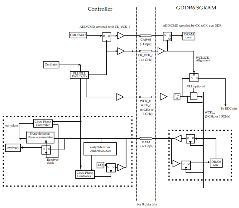
Figure 1 Block diagram [Source]
The Role of GDDR6 in AI and ML
For AI and ML processes, including the training and inference phases, large-scale data processing is necessary. Avoid AI GPUs (Graphics Processing Units) have evolved into the workhorses of AI and ML systems to make sense of this data. The parallel processing capabilities of GPUs are outstanding, which is crucial for addressing the computational demands of workloads for AI and ML.
Data is a crucial piece of information, high-speed memory is needed to store and retrieve massive volumes of data, and GPU performance depends on data analysis. Since the GDDR5 and GDDR5X chips from earlier generations couldn’t handle data transmission speeds more than 12 Gbps/pin, these applications demand faster memory. Here, GDDR6 memory plays a crucial function. AI and ML performance gains require memory to be maintained, hence High Bandwidth Memory (HBM) and GDDR6 offer best-in-class performance in this situation. The Rambus GDDR6 memory subsystem is designed for performance and power efficiency and was created to meet the high-bandwidth, low-latency requirements of AI and ML. The demand for HBM DRAM has significantly increased for gaming consoles and graphics cards as a result of recent developments in artificial intelligence, virtual reality, deep learning, self-driving cars, etc.
Micron’s GDDR6 Memory
Micron’s industry-leading technology enables the next generation faster, smarter global infrastructures, facilitating artificial intelligence (AI), machine learning, and generative AI for gaming. Micron has launched GDDR6X with NVIDIA GeForce® RTX™ 3090 and GeForce® RTX™ 3080 GPUs due to its high-performance computing, higher frame rates, and increased memory bandwidth.
Micron GDDR6 SGRAMs were designed to work with a 1.35V power supply, making them ideal for graphics cards. The memory controller receives a 32-bit wide data interface from GDDR6 devices. GDDR6 employs two channels that are completely independent of one another. A write or read memory access is 256 bits or 32 bytes wide for each channel. Each 256-bit data packet is converted by a parallel-to-serial converter into 16×16-bit data words that are consecutively broadcast via the 16-bit data bus. Originally designed for graphics processing, GDDR6 is a high-performance memory solution that delivers faster data packet processing. GDDR6 supports an IEEE1149.1-2013 compliant boundary scan. Boundary scan allows testing of interconnect on the PCB during manufacturing using state-of-the-art automatic test pattern generation (ATPG) tools.
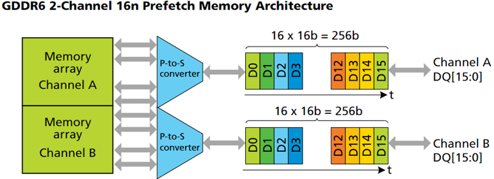
Figure 2 Source
Rambus GDDR6 Memory Interface Subsystem
The JEDEC GDDR6 JESD250C standard is fully supported by the Rambus GDDR6 interface. The Rambus GDDR6 memory interface subsystem fulfills the high-bandwidth, low-latency needs of AI/ML inference and is built for performance and power economy. It includes a PHY and a digital controller that gives users a full GDDR6 memory subsystem. It provides an industry-leading 24 Gb/s per pin and enables two channels with a combined data width of 32 bits. Each channel supports 16 bits. The Rambus GDDR6 interface has a bandwidth of 96GB/s at 24 Gb/s per pin.
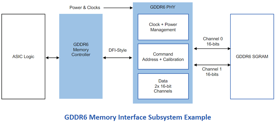
Figure 3 [Source]
Application of GDDR6 memory in AI/ML applications
A large variety of AI/ML applications from many industries employ GDDR6 memory. Here are some actual instances of AI/ML applications that make use of GDDR6 memory:
- FPGA-based AI applications
Micron in their recent new release focused on the development of High-Performance FPGAs based GDDR6 memory for AI applications built on TSMC 7nm process technology with FPGA from Achronix.
2. GDDR6 memory is ideal for AI/ML inference at the edge where fast storage is essential. It offers better memory bandwidth, system speed, and low latency performance, which makes the system to be used for real-time computing of large amounts of data.
3. Advanced driver assistance systems (ADAS)
ADAS employs GDDR6 memory in visual recognition for processing large amounts of visual data, in multiple sensors for tracking and detection, and for real-time decision-making where a large amount of neutral network-based data is analyzed to reduce accidents and for passenger safety.
4. Cloud Gaming
To provide a smooth gaming experience, cloud gaming uses GDDR6 memory, which is fast memory.
5. Healthcare and Medicine:
GDDR6 is used in faster analysis of medical data in the medical industry implemented with AI algorithms for diagnosis and treatment.
IP Trends in GDDR6 use in machine learning and Artificial intelligence
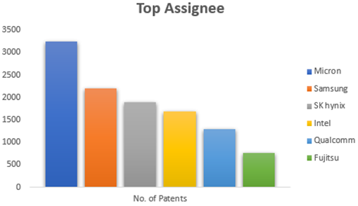
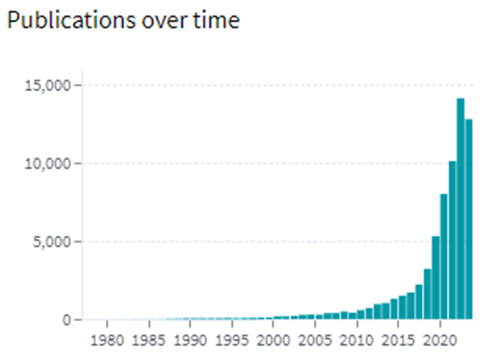
As the importance of high-speed with low latency memory is increasing, there is a significant growth in the patent filing trends witnessed across the globe. The Highest number of patents granted was in 2022 with 212 patents and the highest number of patent applications filed was ~408 in 2022.
INTEL is a dominant player in the market with ~1107 patent families. So far, it has 2.5 times more patent families than NVIDIA Corp., which comes second with 435 patent families. Micron Technology is the third-largest patent holder in the domain.
Other key players in the domain are SK Hynix, Samsung, and AMD.
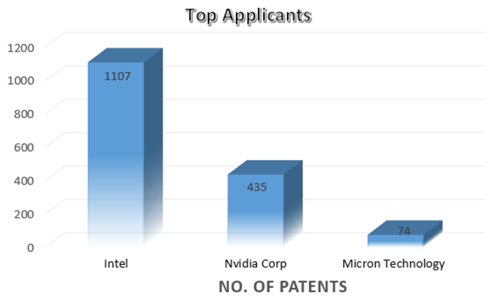
[Source: https://www.lens.org/lens/search/patent/analysis?q=(GDDR6%20memory%20use)]
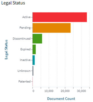
Following are the trends of publication and their legal status over time:
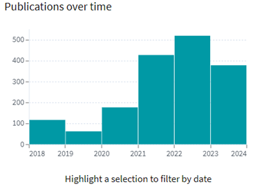

[Source: https://www.lens.org/lens/search/patent/analysis?q=(GDDR6%20memory%20use)]
Conclusion
High-speed memory is a hero who goes unnoticed in the quick-paced world of AI and ML, where every millisecond matters. It has stepped up to the plate, providing great bandwidth, low latency, and enormous capacity, making GDDR6 memory an essential part of AI and ML systems. The IP trends for GDDR6 technology indicate continued attempts to enhance memory solutions for these cutting-edge technologies as demand for AI and ML capabilities rises. These developments bode well for future AI and ML developments, which should become much more amazing.
![High Bandwidth Memory 3 (HBM3): Overcoming Memory Bottlenecks in AI Accelerators With the rise of generative AI models that can produce original text, picture, video, and audio material, artificial intelligence (AI) has made major strides in recent years. These models, like large language models (LLMs), were trained on enormous quantities of data and need a lot of processing power to function properly. However, because of their high cost and processing requirements, AI accelerators now require more effective memory solutions. High Bandwidth Memory, a memory standard that has various benefits over earlier memory technologies, is one such approach. How HBM is relevant to AI accelerators? Constant memory constraints have grown problematic in a number of fields over the past few decades, including embedded technology, artificial intelligence, and the quick growth of generative AI. Since external memory interfaces have such a high demand for bandwidth, several programs have had trouble keeping up. An ASIC (application-specific integrated circuit) often connects with external memory, frequently DDR memory, through a printed circuit board with constrained interface capabilities. The interface with four channels only offers about 60 MB/s of bandwidth even with DDR4 memory. While DDR5 memory has improved in this area, the improvement in bandwidth is still just marginal and cannot keep up with the continuously expanding application needs. However, a shorter link, more channels, and higher memory bandwidth become practical when we take the possibility of high memory bandwidth solutions into account. This makes it possible to have more stacks on each PCB, which would greatly enhance bandwidth. Significant advancements in high memory bandwidth have been made to suit the demands of many applications, notably those demanding complex AI and machine learning models. Latest generation of High Bandwidth Memory The most recent high bandwidth memory standard is HBM3, which is a memory specification for 3D stacked SDRAM that was made available by JEDEC in January 2022. With support for greater densities, faster operation, more banks, enhanced reliability, availability, and serviceability (RAS) features, a lower power interface, and a redesigned clocking architecture, it provides substantial advancements over the previous HBM2E standard (JESD235D). [Source: HBM3 Standard [JEDEC JESD238A] Page 16 of 270] P.S. You can refer to HBM3 Standard [JEDEC JESD238A]: https://www.jedec.org/sites/default/files/docs/JESD238A.pdf for further studies. How does HBM3 address memory bottlenecks in AI accelerators? HBM3 is intended to offer great bandwidth while consuming little energy, making it perfect for AI tasks that need quick and effective data access. HBM3 has a number of significant enhancements over earlier memory standards, including: Increased bandwidth Since HBM3 has a substantially larger bandwidth than its forerunners, data may be sent between the memory and the GPU or CPU more quickly. For AI tasks that require processing massive volumes of data in real-time, this additional bandwidth is essential. Lower power consumption Since HBM3 is intended to be more power-efficient than earlier memory technologies, it will enable AI accelerators to use less energy overall. This is crucial because it may result in considerable cost savings and environmental advantages for data centers that host large-scale AI hardware. Higher memory capacity Greater memory capacities supported by HBM3 enable AI accelerators to store and analyze more data concurrently. This is crucial for difficult AI jobs that need access to a lot of data, such as computer vision or natural language processing. Improved thermal performance AI accelerators are less likely to overheat because to elements in the architecture of HBM3 that aid in heat dissipation. Particularly during demanding AI workloads, this is essential for preserving the system's performance and dependability. Compatibility with existing systems Manufacturers of AI accelerators will find it simpler to implement the new technology because HBM3 is designed to be backward-compatible with earlier HBM iterations without making substantial changes to their current systems. This guarantees an easy switch to HBM3 and makes it possible for quicker integration into the AI ecosystem. In a word, HBM3 offers enhanced bandwidth, reduced power consumption, better memory capacity, improved thermal performance, and compatibility with current systems, making it a suitable memory choice for AI accelerators. HBM3 will play a significant role in overcoming memory constraints and allowing more effective and potent AI systems as AI workloads continue to increase in complexity and size. Intellectual property trends for HBM3 in AI Accelerators HBM3 in AI Accelerators is witnessing rapid growth in patent filing trends across the globe. Over the past few years, the number of patent applications almost getting doubled every two years. MICRON is a dominant player in the market with 50% patents. It now holds twice as many patents as Samsung and SK Hynix combined. Performance, capacity, and power efficiency in today's AI data centers are three areas where Micron's HBM3 Gen2 "breaks new records." It is obvious that the goal is to enable faster infrastructure utilization for AI inference, lower training periods for big language models like GPT-4, and better total cost of ownership (TCO). Other key players who have filed for patents in High bandwidth memory technology with are Intel, Qualcomm, Fujitsu etc. [Source: https://www.lens.org/lens/search/patent/list?q=stacked%20memory%20%2B%20artificial%20intelligence] Following are the trends of publication and their legal status over time: [Source: https://www.lens.org/lens/search/patent/list?q=stacked%20memory%20%2B%20artificial%20intelligence] These Top companies own around 60% of total patents related to UFS. The below diagram shows these companies have built strong IPMoats in US jurisdiction. [Source: https://www.lens.org/lens/search/patent/list?q=stacked%20memory%20%2B%20artificial%20intelligence] Conclusion In summary, compared to earlier memory standards, HBM3 provides larger storage capacity, better bandwidth, reduced power consumption, and improved signal integrity. HBM3 is essential for overcoming memory limitations in the context of AI accelerators and allowing more effective and high-performance AI applications. HBM3 will probably become a typical component in the next AI accelerator designs as the need for AI and ML continues to rise, spurring even more improvements in AI technology. Meta Data The performance of AI accelerators will be improved by the cutting-edge memory technology HBM3, which provides unparalleled data speed and efficiency.](https://intellect-partners.com/wp-content/uploads/2023/12/Blog-Cover-2.png)