Intellect-Partners

Categories
Computer Science

Confidential Computing: Finally Closing That Last Encryption Gap

I remember the first time I really thought about data in use. I was reading a patent application for a healthcare analytics platform, and the diagram showed three neat padlocks: one for data at rest, one for data in transit, and … nothing for the middle step. The middle step was where the server actually crunched the numbers. That gap always bothered me. Why are we comfortable decrypting sensitive data just to do math on it?

Confidential computing is, at heart, the answer to that question. If you’ve been following security trends, you’ve probably heard the phrase “trusted execution environment” or “TEE.” It’s the hardware-backed trick that keeps data encrypted even while the CPU is working on it. I’ve spent enough time reading patent filings around this to realize it isn’t just a buzzword, it’s a genuine shift in how we think about trust in the cloud.

The Encrypted Brain Inside Your Server

The easiest way to picture confidential computing is to imagine a black box inside the processor. You put encrypted data and encrypted code into that box. The box locks itself, decrypts everything internally, processes it, encrypts the result, and only then lets the answer out. The operating system, the hypervisor, even the data center technician with physical access can’t see what’s happening inside. They see only opaque blobs.

Technologies like Intel SGX, AMD SEV-SNP, and ARM CCA make this work at the silicon level. They carve out a region of memory that is hardware-encrypted. The CPU keys are generated inside the processor and never leave. Some people call it “enclave computing” because you are creating a secure enclave in the middle of a potentially hostile environment.

Last year I came across a small startup that was building a tool for banks to jointly screen transactions for sanctions. Without confidential computing, they would have had to move all the data to a neutral third party’s database and hope for the best. With a TEE, the matching algorithm ran entirely inside the enclave. One bank’s raw data never touched the other bank’s raw data, and the cloud provider couldn’t sneak a peek either. That’s a practical trust revolution, not just a theory.

What a Basic Architecture Looks Like

I always find it easier to follow when I can see the moving parts. Here’s a simplified view of a confidential computing setup.

You need a few things to actually build a confidential computing environment. First, a Trusted Execution Environment is the core. That’s the hardware-level secure space. Hardware support is crucial. This isn’t something you can do in software alone. Modern CPUs from Intel (SGX), AMD (SEV), and ARM (TrustZone) have specific instructions and memory protections to create these enclaves.

Encryption is obviously there data stays encrypted throughout. But unlike traditional encryption, the keys are handled inside the enclave, so even the hypervisor or cloud provider doesn’t have access. Remote attestation is a less talked about but really important piece. It’s a way for you to verify that the code running inside the enclave is exactly what you expect, and hasn’t been tampered with. You can basically ask the hardware to prove the enclave is legitimate.

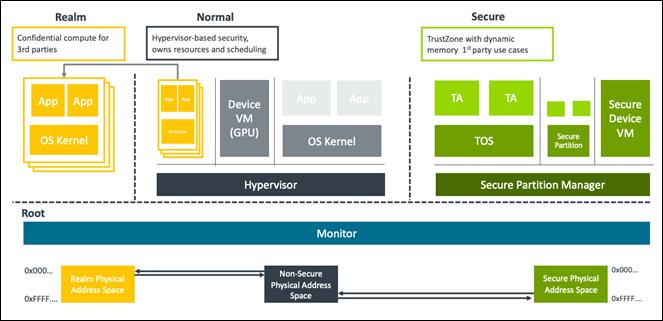
At the base, you have the cloud infrastructure you don’t fully trust. Sitting inside it is the enclave, which is a locked memory region. The application and its data enter encrypted. Before anything runs, an attestation handshake happens: the enclave generates a cryptographic quote proving it’s a genuine hardware enclave running unmodified code. A remote attestation service verifies that quote. Only if the check passes does the data decryption key get released to the enclave. The whole time, the cloud provider’s staff can’t access the plaintext.

This architecture changes the shared responsibility model. You no longer need to trust the cloud provider’s entire software stack. You still have to trust Intel or AMD to have built the hardware correctly, but that’s a far smaller circle.

Places It’s Quietly Making a Difference

Most headlines focus on confidential computing for financial services or healthcare, and that’s fair. But I’ve seen interesting use cases pop up in places that don’t make the evening news.

One is software IP protection. A company selling a machine-learning model to a factory can deliver it inside an enclave. The factory runs inference on their own sensitive production data, but they can’t extract the model weights. The seller’s intellectual property stays locked even while running on someone else’s hardware. That solves a huge licensing headache.

Another is in multi-party research. Pharmaceutical companies hate sharing raw compound data with competitors, but they do want to know if their molecules interact with similar protein targets. A confidential computing cluster can run simulations on pooled encrypted data and output only the interaction scores. No raw molecule structures get exposed.

Wearables and edge devices will likely follow. If my smartwatch could process heart rhythm anomalies in a small enclave and share only a verified alert with my doctor, I’d feel much better about privacy. The enclave could even prove mathematically that it followed the diagnostic algorithm exactly, without revealing raw waveform data.

Why It’s Not Yet Everywhere

Truthfully, confidential computing is still a bit fiddly. Performance overhead used to be punishing, though it has improved a lot. Enclave memory was tiny in the early Intel SGX days and trying to fit a large database index inside an enclave was like filling a suitcase with an elephant. You had to swap encrypted pages constantly, and that slowed things down. AMD’s SEV encrypts entire virtual machines with less pain, but you still need to benchmark your specific workload.

Attestation is another beast. Setting up a trustworthy attestation service and managing certificates across different clouds is no joke. And side-channel attacks, while highly sophisticated, are not science fiction. There’s a constant cat-and-mouse game between researchers and chip vendors.

Then there’s the human angle. If you write buggy code inside the enclave, the hardware will faithfully execute every vulnerability for you. The enclave isn’t a code reviewer. It just guarantees that no one outside can read the memory. Garbage code inside still produces garbage, or worse, leaks.

Where I Think It’s Headed

I suspect confidential computing will become boring in five years, which is the best compliment you can give a security technology. Cloud providers already offer it as a checkbox on certain VM types. Kubernetes operators for confidential containers are maturing. The Confidential Computing Consortium keeps pushing for open standards so that you can move an enclave workload across clouds without a rewrite.

The real magic will happen when confidential computing pairs with other privacy techniques and maybe combine it with federated learning so that local models share updates through an enclave that can’t snoop on individual contributions. That’s the kind of architecture that will finally make privacy regulations and innovative data sharing coexist without an endless legal battle.

For now, the idea that a server can process data it cannot read feels almost magical. But it’s real silicon and real code. It finally plugs that middle padlock. And for anyone thinking about the next generation of trustworthy computing, it’s the foundation we should be building on.

For a long time, protecting data at rest and in transit was considered good enough. But as we move toward more shared infrastructure and data-driven applications, the gap during processing has become too big to ignore. Confidential computing fills that gap. It lets you process sensitive data without exposing it is not even to the platform running it. That changes the trust model for cloud computing, multi-party analytics, and pretty much anything involving sensitive data in shared environments.

The technology is still maturing. Performance and usability need to improve. But I think it’s going to become a standard part of security architecture over the next few years, especially in regulated industries where data privacy isn’t optional.

Categories
Computer Science Electronics

Popular microcontrollers and their architecture

Microcontrollers

A microcontroller is a programmable processing element with an embedded memory system and multiple programmable input and output peripherals. The peripherals can be advanced GPU, coprocessors, or other electronic components. Microcontrollers are used in different electronic devices for implementing various applications.

It can be used in the device, which can be automatically controlled. Further, it is mostly used in automobiles, computer systems, and different appliances

There are multiple manufacturers of microcontrollers in the market. Such as 

  1. Cypress Semiconductor
  2. NXP Semiconductor
  3. Silicon labs
  4. ARM
  5. MIPS
  6. Maxim Integrated
  7. Renesas
  8. Intel 
  9. Microchip technology

we will learn about the different components of the popular microcontrollers from three manufacturers.

Texas Instrument C2000 MCU

Texas Instrument makes multiple products ranging from all electronic devices, including MCUs. Different MCUs being produced by Texas Instruments are ARM-based MCUs, C2000 MCUs, DSPs, and MSP430 microcontrollers. The most popular MCUs of Texas Instruments are C200 MCUs, used in various electronic devices to perform different control operations, such as digital power and motor control.

C2000 MCUs:

Each C2000 MCU is a combination of multiple configurable blocks that are interconnected. Each CLC can be configured to perform custom operations as per configuration information.

Feature of C2000 Microcontrollers:

1. It provides high computational capabilities with an advanced floating-point data processing unit. 

2. It implements a highly accurate ADC converter

3. It implements integrated comparators for performing comparison operations. 

4. It implements a very high communication interface for the communication of signals and data.

Implementation of C2000 Microcontrollers

Implementation of C2000 Microcontrollers:

The microcontroller can help us to make independent custom logic units to perform different custom logical operations. The MCUs implement multiple Configurable Logic Cells (CLC) in the system, which can be configured or programmed for custom operations. Multiple custom logical units are connected using different local or Universal buses. Each CLC is associated with a PWM module for powering up the CLC. The global bus further connects multiple CLBs.

The input of one CLB can be inputted to another CLB to create a cascading effect.

CLB System Arhitecture
CLB unit modules and CLB sub-modules

Each CLB unit includes multiple CLB sub-modules, namely:

  1. 4-Input Look-up table (LUT) submodules – LUT unit helps to create any boolean operations using up to 4 inputs
  2. 4-State Finite State Machine (FSM) – 4-State FSM generates up to 4 states based on input received.
  3. Counter unit – The counter can act as a counter, shifter, or adder. As a counter, it can count up or down; as a shifter, it can shift right or left; as an adder, it can add or subtract. 
  4. Output Look-up table (LUT) – The output LUT can be configured with boolean operations. 
  5. High-Level Controller (HLC) – The HLC can perform different control operations in the system. The HLC performs data exchange or interrupt operations.
TMS320F28004x Real-Time Microcontrollers

Link to documentation of TI C2000 MCUs are:

https://www.ti.com/microcontrollers-mcus-processors/c2000-real-time-control-mcus/overview.html

https://www.ti.com/lit/ml/slyp681/slyp681.pdf?ts=1655705809321&ref_url=https%253A%252F%252Fwww.google.com%252F

https://www.ti.com/lit/an/spracn0f/spracn0f.pdf?ts=1702390944874

https://www.ti.com/lit/ug/spruii0e/spruii0e.pdf?ts=1702390956144

https://www.ti.com/lit/ug/spruin7b/spruin7b.pdf?ts=1702390972904

NXP S32V2 Processors

NXP has been active in the microcontroller market for a long time. NXP S32V2 MCUs form vision processors for processing images using its APEX-2 vision accelerators in sensing apparatus. It offers an image signal processor and a 3D graphics processing unit (GPU). They are extensively used in ADAS to detect object and image recognition operations.

S32V2 Processor:

The MCU features an APEX-2 vision accelerator for implementing image processing operations using the APEX core framework and an APEX graph tool for sensing different objects ahead of it. The NXP MCu has been implemented in the Bluebox engine for autonomous driving.

Implementation of S32V2 Processor:

  1. Cortex processor A53 for processing different inputs.
  2. APEX-2 vision accelerators:
  3. GPU and Hardware security encryption mechanism
  4. Fabric and internal memory
APEX-2 vision accelerators: GPU and Hardware security encryption mechanism Fabric and internal memory

The APEX processing unit implements two APUs and 16 computational units (CU), and each CU includes four functional units: Multiplier, Load-store, ALU, and shifter unit. 

Each APU is a parallel processor for processing different computational operations. The APU manages the execution and data movement by dispatching instructions to different CUs. 

It has been extensively used in 3D content creation, advanced driver assistance, and video surveillance for recognizing different objects. And people.

G2-APEX-642 ICP Core
APEX ICP Core - Data Flow Management & HW Acceleration

The ACP is a 32-bit RISCV-based processor. The APU implements both scaler and SIMD capabilities. The scaler processing is performed in the Array control processor (ACP) unit. Vector processing is done at the Vector processing unit.

S32V234 Vision Processor - Architecture

Link to documentation of NXP S32V2 MCUs are:

https://www.nxp.com/products/processors-and-microcontrollers/arm-processors/s32-automotive-processors/s32v2-processors-for-vision-machine-learning-and-sensor-fusion:S32V234

https://www.nxp.com/docs/en/data-sheet/S32V234.pdf

https://www.nxp.com/webapp/Download?colCode=S32V234RM

Silabs EFM8 Busy Bee MCU

Silicon Labs’s Laser Bee MCU includes analog-intensive MCUs. This MCU offers high computational operations, including 14-bit ADC, temperature sensors, and high-speed communication peripherals in packages.

Silabs EFM8 Busy Bee MCU

Implementation of Silabs EFM8 Busy Bee:

  1. It includes up to four configurable logic cells.
  2. They are used in different apps and locations that require programmable operations.
  3. Each unit supports 256 other combinational logic functions. Such as AND, OR, XOR, and multiplexing.
  4. Each CLU has a look-up logic (LUT) logic function that can be used to perform 256 different operations. Each CLU contains a D flip-flop, whose input is the LUT output. Multiple CLUs can be cascaded together to achieve some functions.
Silabs EFM8 Busy Bee Architecture

Link to documentation of TI C2000 MCUs are:

https://www.silabs.com/mcu/8-bit-microcontrollers/efm8-laser-bee

https://www.silabs.com/documents/public/training/mcu/em8-mcu-overview.pdf

https://www.silabs.com/mcu/8-bit-microcontrollers/efm8-bb5

https://www.silabs.com/documents/public/application-notes/AN921.pdf

https://www.silabs.com/documents/public/training/mcu/efm8-lb1-clu.pdf

Categories
Computer Science

Powering AI and ML: Unveiling GDDR6’s Role in High-Speed Memory Technology

Introduction

Artificial intelligence (AI) and machine learning (ML) have evolved into game-changing technologies with limitless applications ranging from natural language processing to the automobile sector. These applications need a significant amount of computing power, and memory is an often neglected resource. Fast memory is crucial for AI and ML activities, and GDDR6 memory has established itself as a prominent participant in this industry where high speed and computing power are necessary. The following article will investigate the usage of GDDR6 in AI and ML applications, as well as current IP trends in this crucial subject.

Architecture of GDDR6

High-speed dynamic random-access memory with high bandwidth requirements is the GDDR6 DRAM. The high-speed interface of the GDDR6 SGRAM is designed for point-to-point communications to a host controller. To accomplish high-speed operation, GDDR6 employs a 16n prefetch architecture and a DDR or QDR interface. The architecture of the technology has two 16-bit wide, completely independent channels.

GDDR6 Controller SGRAM

Figure 1 Block diagram [Source]

The Role of GDDR6 in AI and ML

For AI and ML processes, including the training and inference phases, large-scale data processing is necessary. Avoid AI GPUs (Graphics Processing Units) have evolved into the workhorses of AI and ML systems to make sense of this data. The parallel processing capabilities of GPUs are outstanding, which is crucial for addressing the computational demands of workloads for AI and ML.

Data is a crucial piece of information, high-speed memory is needed to store and retrieve massive volumes of data, and GPU performance depends on data analysis. Since the GDDR5 and GDDR5X chips from earlier generations couldn’t handle data transmission speeds more than 12 Gbps/pin, these applications demand faster memory. Here, GDDR6 memory plays a crucial function. AI and ML performance gains require memory to be maintained, hence High Bandwidth Memory (HBM) and GDDR6 offer best-in-class performance in this situation. The Rambus GDDR6 memory subsystem is designed for performance and power efficiency and was created to meet the high-bandwidth, low-latency requirements of AI and ML. The demand for HBM DRAM has significantly increased for gaming consoles and graphics cards as a result of recent developments in artificial intelligence, virtual reality, deep learning, self-driving cars, etc.

Micron’s GDDR6 Memory

Micron’s industry-leading technology enables the next generation faster, smarter global infrastructures, facilitating artificial intelligence (AI), machine learning, and generative AI for gaming. Micron has launched GDDR6X with NVIDIA GeForce® RTX™ 3090 and GeForce® RTX™ 3080 GPUs due to its high-performance computing, higher frame rates, and increased memory bandwidth.

Micron GDDR6 SGRAMs were designed to work with a 1.35V power supply, making them ideal for graphics cards. The memory controller receives a 32-bit wide data interface from GDDR6 devices. GDDR6 employs two channels that are completely independent of one another. A write or read memory access is 256 bits or 32 bytes wide for each channel. Each 256-bit data packet is converted by a parallel-to-serial converter into 16×16-bit data words that are consecutively broadcast via the 16-bit data bus. Originally designed for graphics processing, GDDR6 is a high-performance memory solution that delivers faster data packet processing. GDDR6 supports an IEEE1149.1-2013 compliant boundary scan. Boundary scan allows testing of interconnect on the PCB during manufacturing using state-of-the-art automatic test pattern generation (ATPG) tools.

GDDR6 2-channel 16n Prefetch Memory Architecture

Figure 2 Source

Rambus GDDR6 Memory Interface Subsystem

The JEDEC GDDR6 JESD250C standard is fully supported by the Rambus GDDR6 interface. The Rambus GDDR6 memory interface subsystem fulfills the high-bandwidth, low-latency needs of AI/ML inference and is built for performance and power economy. It includes a PHY and a digital controller that gives users a full GDDR6 memory subsystem. It provides an industry-leading 24 Gb/s per pin and enables two channels with a combined data width of 32 bits. Each channel supports 16 bits. The Rambus GDDR6 interface has a bandwidth of 96GB/s at 24 Gb/s per pin.

GDDR6 Memory Interface Subsystem Example

Figure 3 [Source]

Application of GDDR6 memory in AI/ML applications

A large variety of AI/ML applications from many industries employ GDDR6 memory. Here are some actual instances of AI/ML applications that make use of GDDR6 memory:

  1. FPGA-based AI applications

Micron in their recent new release focused on the development of High-Performance FPGAs based GDDR6 memory for AI applications built on TSMC 7nm process technology with FPGA from Achronix.

2. GDDR6 memory is ideal for AI/ML inference at the edge where fast storage is essential. It offers better memory bandwidth, system speed, and low latency performance, which makes the system to be used for real-time computing of large amounts of data.

3. Advanced driver assistance systems (ADAS)

ADAS employs GDDR6 memory in visual recognition for processing large amounts of visual data, in multiple sensors for tracking and detection, and for real-time decision-making where a large amount of neutral network-based data is analyzed to reduce accidents and for passenger safety.

4. Cloud Gaming

To provide a smooth gaming experience, cloud gaming uses GDDR6 memory, which is fast memory.

5. Healthcare and Medicine:

GDDR6 is used in faster analysis of medical data in the medical industry implemented with AI algorithms for diagnosis and treatment.

IP Trends in GDDR6 use in machine learning and Artificial intelligence

As the importance of high-speed with low latency memory is increasing, there is a significant growth in the patent filing trends witnessed across the globe. The Highest number of patents granted was in 2022 with 212 patents and the highest number of patent applications filed was ~408 in 2022.

INTEL is a dominant player in the market with ~1107 patent families. So far, it has 2.5 times more patent families than NVIDIA Corp., which comes second with 435 patent families. Micron Technology is the third-largest patent holder in the domain.

Other key players in the domain are SK Hynix, Samsung, and AMD.

Top Applicants for GDDR6 Memory Use

[Source: https://www.lens.org/lens/search/patent/analysis?q=(GDDR6%20memory%20use)]

Following are the trends of publication and their legal status over time:

publication status over time
Legal status over time

[Source: https://www.lens.org/lens/search/patent/analysis?q=(GDDR6%20memory%20use)]

Conclusion

High-speed memory is a hero who goes unnoticed in the quick-paced world of AI and ML, where every millisecond matters. It has stepped up to the plate, providing great bandwidth, low latency, and enormous capacity, making GDDR6 memory an essential part of AI and ML systems. The IP trends for GDDR6 technology indicate continued attempts to enhance memory solutions for these cutting-edge technologies as demand for AI and ML capabilities rises. These developments bode well for future AI and ML developments, which should become much more amazing.