Categories
Electronics Others

Migration from Hybrid Memory Cube (HMC) to High-Bandwidth Memory (HBM)

Introduction:

Memory technology plays a vital role in providing effective data processing as the demand for high-performance computing keeps rising. The industry has recently seen a considerable migration from Hybrid Memory Cube (HMC) to High-Bandwidth Memory (HBM) because of HMB’s higher performance, durability, and scalability. This technical note talks about the causes behind the widespread adoption of HBM as well as the benefits it has over HMC.

HBM Overview:

HBM is a revolutionary memory technology that outperforms conventional memory technologies. HBM is a vertically stacked DRAM memory device interconnected to each other using through-silicon vias (TSVs). HBM DRAM die is further tightly connected to the host device using its distribution channels which are completely independent of one another. This architecture is used to achieve high-speed, low-power operation. HBM has a reduced form factor because it combines DRAM dies and logic dies in a single package, making it ideal for space-constrained applications. An interposer that is interconnected to the memory stacks, enables high-speed data transmission between memory and processor units. 

HMC Brief:

The Hybrid Memory Cube (HMC) comprises multiple stacked DRAM dies and a logic die, stacked together using through-silicon via (TSV) technology in a single-package 3D-stacked memory device. The HMC stack’s memory dies each include their memory banks as well as a logic die for memory access control. It was developed by Micron Technology and Samsung Electronics Co. Ltd. in 2011, and announced by Micron in September 2011.

When compared to traditional memory architectures such as DDR3, it enables faster data access and lower power consumption. Each memory in HMC is organized into a vault. Each vault in the logic die has a memory controller which manages memory operations. HMC is used in applications where speed, bandwidth, and sizes are more required. Micron discontinued the use of HMC in 2018 when it failed to become successful in the semiconductor industry.

Hybrid Memory Cube (HMC) and High-Bandwidth Memory (HBM) are two distinct memory technologies that have made significant contributions to high-performance computing. While both of these technologies aim to enhance memory bandwidth operation, there are many fundamental distinctions between HMC and HBM.

Power Consumption: HBM significantly has lower power consumption compared to HMC. HBM’s vertical stacking approach eliminates high-power consumption bus interfaces and reduces the distance for data transfer between DRAM dies, resulting in improved energy efficiency. This decreased power usage is especially beneficial in power-constrained environments like mobile devices or energy-efficient servers.

Memory Architecture: HMC uses a 3D-stacked memory device comprised of several DRAM dies and a logic die stacked together via through-silicon (TSV) technology. In addition to its memory banks, each memory die in the HMC stack contains a logic die for a memory access operation. HBM, on the other hand, is a 3D-stacked architecture that integrates base (logic) die and memory dies as well as a processor (GPU) on a single package that is coupled by TSVs to provide a tightly coupled high-speed processing unit. The memory management process is made easier by the shared memory space shared by the memory dies in an HBM stack.

Industry Adoption: When compared to HMC, HBM offers more memory density in a smaller physical footprint. HBM does this by vertically stacking memory dies on a single chip, resulting in increased memory capacity in a smaller form factor. HBM is well-suited for space-constrained applications such as graphics cards and mobile devices because of its density.

Memory Density: In comparison to HMC, HBM frequently utilizes less energy and power. The vertical stacking strategy used by HBM shortens the transfer of data distance and removes power-hungry bus connections, resulting in increased energy efficiency. This decreased power usage is especially beneficial in power-constrained contexts like mobile devices or energy-efficient servers.

Memory Bandwidth: Comparing HMC and HBM to conventional memory technologies, they both offer much better memory bandwidth. On the other hand, HBM often delivers higher bandwidth compared to HMC. By using a wider data channel and higher signaling rates, HBM accomplishes this, enabling faster data flow between the processor and the memory units.

In conclusion, HMC and HBM differ in terms of memory bandwidth, architecture, power consumption, density, and industry recognition. While HMC offers significantly better performance over conventional memory technologies, HBM has become the market leader due to its reduced form factor, higher performance, and efficiency, which has expedited the transition from HMC to HBM.

Advantages of HBM:

Power Consumption: HBM uses less energy and power for data transfer on the I/O interface than HMC, hence lowering energy efficiency. HBM improves energy efficiency by using vertical stacking technology to reduce data transfer distance and power-intensive bus interfaces.

Bandwidth: HBM provides excellent memory bandwidth, allowing the processor/controller to quickly access data to obtain greater speed. HBM has more memory channels and along with high-speed signaling than HMC, which allows for more bandwidth. This high bandwidth is critical for data-intensive applications such as AI, machine learning, and graphics.

Scalability: By enabling the connection of different memory stacks, HBM offers scalable memory configurations. Because of this flexibility, numerous memory and bandwidth options are available to meet the unique needs of various applications.

Density: With a reduced size, HBM’s vertical stacking technique makes greater memory densities possible. HBM memory is ideal for smaller devices such as mobile phones and graphics cards etc. Enhanced system performance is also made possible by higher memory density by lowering data access latency.

Signal Integrity: TSV-based interconnects in HBM provide superior signal integrity than wire-bonded techniques. The reduced data transmission failures and increased system dependability are both benefits of improved signal integrity.

Conclusion:

A significant development in memory technology is the change from HMC to HBM. The requirement for faster and more effective memory solutions has been spurred by the demand for high-performance computing, particularly in fields like AI, machine learning, and graphics. With its different benefits, HBM is broadly utilized in various ventures because of its high bandwidth, low power consumption, increased density, versatility, and improved signal integrity. HBM has become the standard option for high-performance memory needs, and its continuous development is expected to influence the direction of memory technologies in the market.

Categories
Computer Science

Understanding UFS WriteBooster: The Power Behind Enhanced Memory Performance

SIGNIFICANCE OF WRITEBOOSTER IN UFS

A flash storage specification for digital cameras, cell phones, and other consumer electronics is called Universal Flash Storage (UFS). The 8-lane parallel and half-duplex LVDS interface of eMMCs cannot scale to larger bandwidths as well as the full-duplex serial LVDS interface implemented by UFS. The UFS standard was updated to version 3.1 by JEDEC in January 2020, adding features including Write Booster, Deep Sleep, Performance Throttling Notification, and Host Performance Booster. The significance of WriteBooster mode in UFS and its application to enhancing memory performance will be covered in this essay.

What is WriteBooster mode?

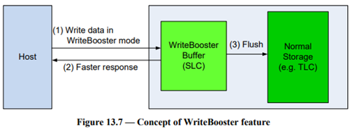
This feature enables UFS storage devices to use a portion of the flash as a pseudo-SLC cache to increase writing performance. This feature enhances the write performance of UFS storage devices, making them faster and more effective, while creating a reserve memory in the flash storage that is easily and frequently accessible. It uses very little space (only 1 bit of data in each cell). Additionally, WriteBooster is a more affordable option that offers comparable performance advantages.

Operation process of WriteBooster mode

The WriteBooster mode in UFS devices operates as follows:

Pseudo SLC Cache

When using WriteBooster mode, flash storage is created with a reserve memory that serves as a pseudo-SLC cache. In the flash storage, this cache is designed to serve as a frequently accessible reserve memory. Just 1 bit of data is stored in each cell, taking up extremely little space while improving write performance.

Write Acceleration

Data is first written to the WriteBooster mode-created pseudo-SLC cache before being written to the UFS storage device. As opposed to writing directly to the flash memory, writing to this cache is quicker. The device can swiftly complete write operations and move on to other activities thanks to the cache’s function as a buffer.

Background Flushing

In the background, the information kept in the pseudo-SLC cache is periodically flushed to the flash memory. By doing this, you may retain the device’s rapid write rates for following operations while also making sure the data is permanently recorded in the flash memory.

Benefits for Performance

WriteBooster mode enhances the write performance of UFS devices by utilizing the pseudo-SLC cache. As a result, write speeds increase, which can speed up application launch, cache loading, browsing performance, and encoding times. Additionally, the feature enhances the responsiveness and general performance of the system.   

NOTE: It’s important to keep in mind that the exact UFS device and how it’s implemented may affect whether WriteBooster mode can be enabled or disabled. Disabling WriteBooster mode would result in write operations proceeding as normal writes, without utilizing the pseudo-SLC cache.  

Benefits of WriteBooster mode

There are a number of advantages to WriteBooster mode being used with UFS:

Faster Write Speeds

Using a pseudo-SLC cache, WriteBooster mode on UFS devices increases write speeds. Because of the cache, write operations can be completed more quickly, which decreases the amount of time the device needs to be active. The device can reach low-power modes as a result more quickly, increasing power efficiency.

Better Memory Management

By using a piece of the flash as a fictitious SLC cache, WriteBooster mode in UFS improves memory management. Because of the cache, write operations can be completed more quickly, which decreases the amount of time the device needs to be active. The device can reach low-power modes as a result more quickly, increasing power efficiency.

Affordable Alternative

WriteBooster mode in UFS offers comparable performance advantages to pSLC Write Buffer at a lesser price. As a result, it offers a viable option for enhancing memory performance in UFS devices.

Impact of WriteBooster mode on UFS’s power usage

The following ways that WriteBooster mode in UFS affects power usage:

Power Efficiency

By streamlining the writing process, UFS’ Write Booster mode helps to increase power efficiency. The device can write data more quickly and cut down on the time needed for write operations by using a pseudo-SLC cache. As a result, write operations consume less power since the device can perform them more rapidly and effectively.

Deep Sleep Mode

In addition to WriteBooster mode, UFS 3.1 also introduces the Deep Sleep feature. By using voltage regulators for storage and other purposes in addition to power reduction, deep sleep mode reduces energy usage. This improves overall power efficiency by enabling the device to use less power when it is idle or in low-power modes.   

Effective Memory Management

Using a piece of the flash as a fictitious SLC cache, WriteBooster mode in UFS improves memory management. Because of the cache, write operations can be completed more quickly, which decreases the amount of time the device needs to be active. The device can reach low-power modes as a result more quickly, increasing power efficiency.

Overall, WriteBooster mode in UFS reduces power usage through write process optimization, the use of a pseudo-SLC cache, and the addition of features like Deep Sleep mode. Through these improvements, devices can write operations more quickly and use less power whether they are idle or in low-power states.

Intellectual property trends for WriteBooster mode in UFS

WriteBooster mode in UFS is witnessing rapid growth in patent filing trends across the globe. Over the past few years, the number of patent applications almost doubled every two years.    

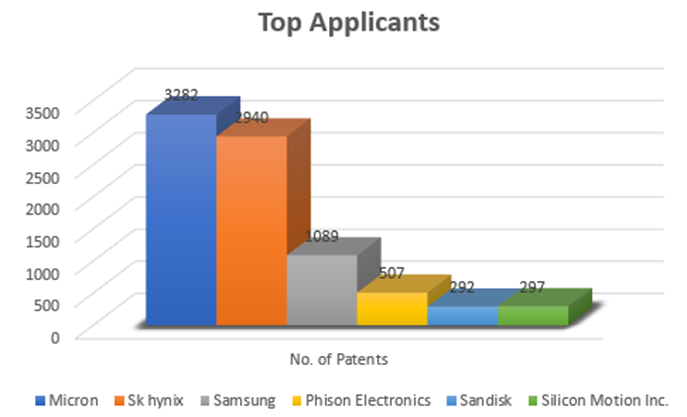
MICRON is a dominant player in the market with ~3282 patents. So far, it has 2 times more patents than Samsung.

Other key players who have filed for patents in UFS technology with SLC NAND are Sk Hynix, Sandisk, Western Digital etc.  

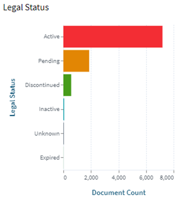
Following are the trends of publication and their legal status over time:

trends of publication and their legal status over time

These Top 10 companies own around 60% of total patents related to UFS. The below diagram shows these companies have built strong IPMoats in US jurisdiction.  

Conclusion

In conclusion, WriteBooster mode is a crucial component of UFS that boosts write speeds to enhance memory performance. Faster write rates, a pseudo-SLC cache that is easily and repeatedly accessible reserve memory in the flash storage, and a cost-effective solution that offers comparable performance benefits as pSLC Write Buffer are only a few advantages of the implementation of WriteBooster mode in UFS. The significance of UFS’ WriteBooster mode will only increase as mobile devices become more potent and feature-rich. Although Write Booster mode’s effectiveness on UFS devices may vary depending on the specific device, the function is intended to increase write speeds and memory performance, which leads to quicker app startup times, quicker file transfers, and greater system responsiveness.