Microcontrollers
A microcontroller is a programmable processing element with an embedded memory system and multiple programmable input and output peripherals. The peripherals can be advanced GPU, coprocessors, or other electronic components. Microcontrollers are used in different electronic devices for implementing various applications.
It can be used in the device, which can be automatically controlled. Further, it is mostly used in automobiles, computer systems, and different appliances.
There are multiple manufacturers of microcontrollers in the market. Such as
- Cypress Semiconductor
- NXP Semiconductor
- Silicon labs
- ARM
- MIPS
- Maxim Integrated
- Renesas
- Intel
- Microchip technology
we will learn about the different components of the popular microcontrollers from three manufacturers.
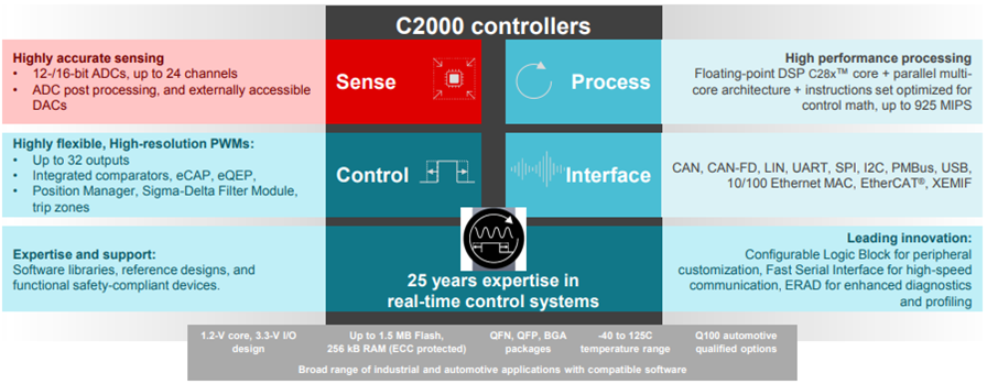
Texas Instrument C2000 MCU
Texas Instrument makes multiple products ranging from all electronic devices, including MCUs. Different MCUs being produced by Texas Instruments are ARM-based MCUs, C2000 MCUs, DSPs, and MSP430 microcontrollers. The most popular MCUs of Texas Instruments are C200 MCUs, used in various electronic devices to perform different control operations, such as digital power and motor control.
C2000 MCUs:
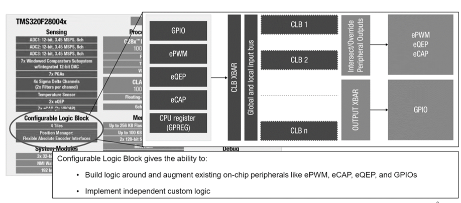
Each C2000 MCU is a combination of multiple configurable blocks that are interconnected. Each CLC can be configured to perform custom operations as per configuration information.
Feature of C2000 Microcontrollers:
1. It provides high computational capabilities with an advanced floating-point data processing unit.
2. It implements a highly accurate ADC converter.
3. It implements integrated comparators for performing comparison operations.
4. It implements a very high communication interface for the communication of signals and data.
Implementation of C2000 Microcontrollers:
The microcontroller can help us to make independent custom logic units to perform different custom logical operations. The MCUs implement multiple Configurable Logic Cells (CLC) in the system, which can be configured or programmed for custom operations. Multiple custom logical units are connected using different local or Universal buses. Each CLC is associated with a PWM module for powering up the CLC. The global bus further connects multiple CLBs.
The input of one CLB can be inputted to another CLB to create a cascading effect.
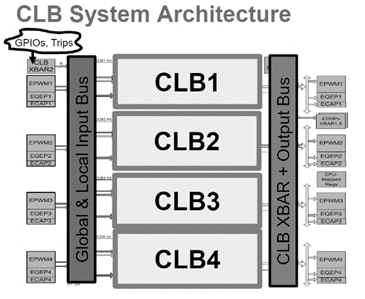
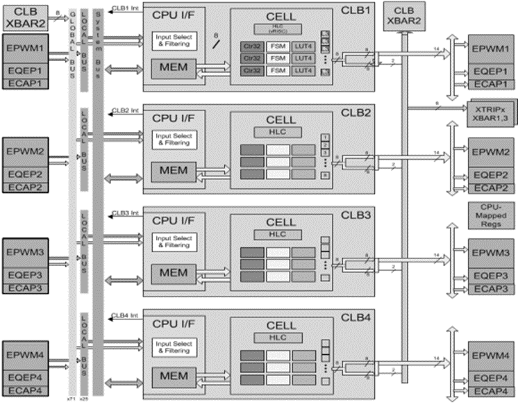
Each CLB unit includes multiple CLB sub-modules, namely:
- 4-Input Look-up table (LUT) submodules – LUT unit helps to create any boolean operations using up to 4 inputs
- 4-State Finite State Machine (FSM) – 4-State FSM generates up to 4 states based on input received.
- Counter unit – The counter can act as a counter, shifter, or adder. As a counter, it can count up or down; as a shifter, it can shift right or left; as an adder, it can add or subtract.
- Output Look-up table (LUT) – The output LUT can be configured with boolean operations.
- High-Level Controller (HLC) – The HLC can perform different control operations in the system. The HLC performs data exchange or interrupt operations.
Link to documentation of TI C2000 MCUs are:
https://www.ti.com/microcontrollers-mcus-processors/c2000-real-time-control-mcus/overview.html
https://www.ti.com/lit/an/spracn0f/spracn0f.pdf?ts=1702390944874
https://www.ti.com/lit/ug/spruii0e/spruii0e.pdf?ts=1702390956144
https://www.ti.com/lit/ug/spruin7b/spruin7b.pdf?ts=1702390972904
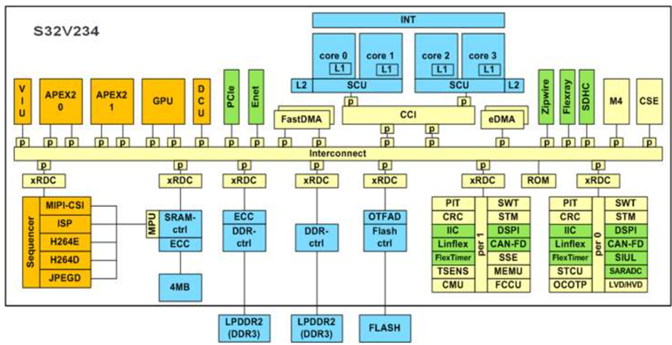
NXP S32V2 Processors
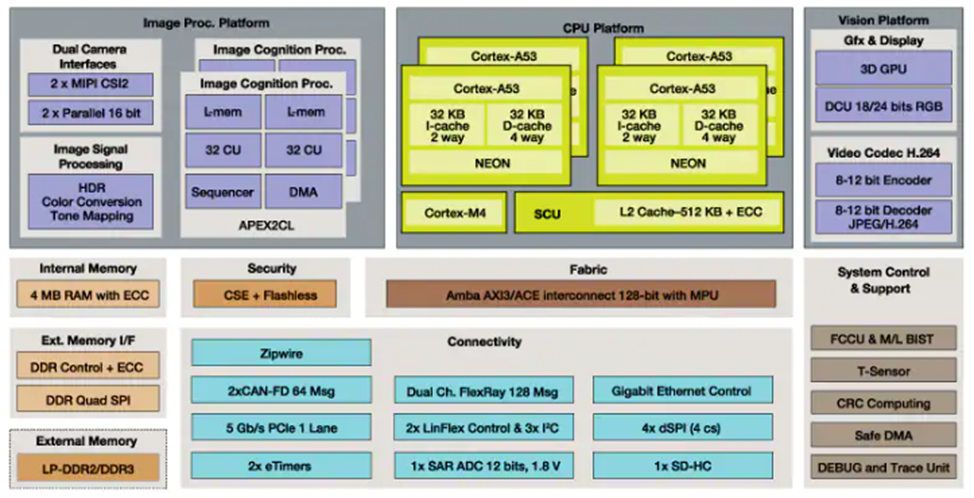
NXP has been active in the microcontroller market for a long time. NXP S32V2 MCUs form vision processors for processing images using its APEX-2 vision accelerators in sensing apparatus. It offers an image signal processor and a 3D graphics processing unit (GPU). They are extensively used in ADAS to detect object and image recognition operations.
S32V2 Processor:
The MCU features an APEX-2 vision accelerator for implementing image processing operations using the APEX core framework and an APEX graph tool for sensing different objects ahead of it. The NXP MCu has been implemented in the Bluebox engine for autonomous driving.
Implementation of S32V2 Processor:
- Cortex processor A53 for processing different inputs.
- APEX-2 vision accelerators:
- GPU and Hardware security encryption mechanism
- Fabric and internal memory
The APEX processing unit implements two APUs and 16 computational units (CU), and each CU includes four functional units: Multiplier, Load-store, ALU, and shifter unit.
Each APU is a parallel processor for processing different computational operations. The APU manages the execution and data movement by dispatching instructions to different CUs.
It has been extensively used in 3D content creation, advanced driver assistance, and video surveillance for recognizing different objects. And people.
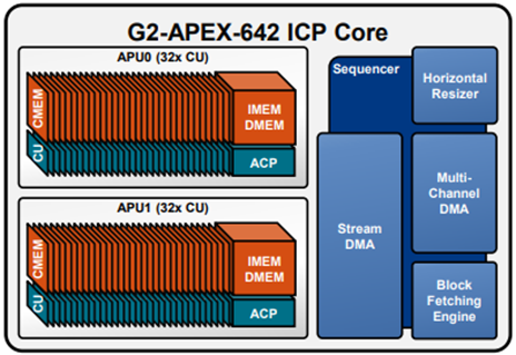
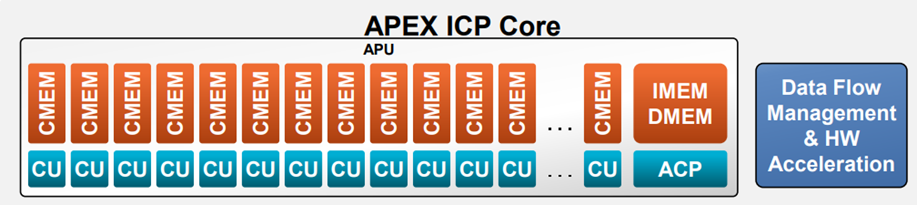
The ACP is a 32-bit RISCV-based processor. The APU implements both scaler and SIMD capabilities. The scaler processing is performed in the Array control processor (ACP) unit. Vector processing is done at the Vector processing unit.
Link to documentation of NXP S32V2 MCUs are:
https://www.nxp.com/docs/en/data-sheet/S32V234.pdf
https://www.nxp.com/webapp/Download?colCode=S32V234RM
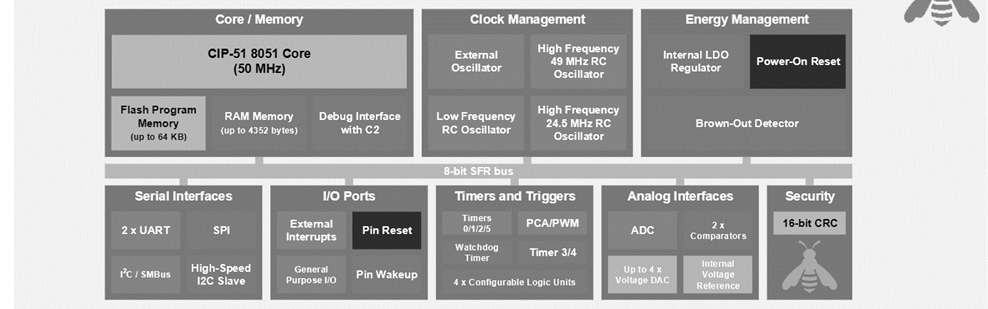
Silabs EFM8 Busy Bee MCU
Silicon Labs’s Laser Bee MCU includes analog-intensive MCUs. This MCU offers high computational operations, including 14-bit ADC, temperature sensors, and high-speed communication peripherals in packages.
Implementation of Silabs EFM8 Busy Bee:
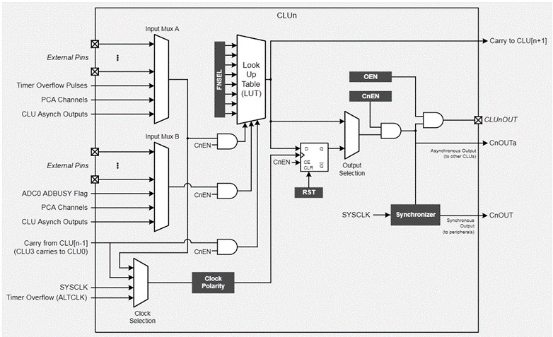
- It includes up to four configurable logic cells.
- They are used in different apps and locations that require programmable operations.
- Each unit supports 256 other combinational logic functions. Such as AND, OR, XOR, and multiplexing.
- Each CLU has a look-up logic (LUT) logic function that can be used to perform 256 different operations. Each CLU contains a D flip-flop, whose input is the LUT output. Multiple CLUs can be cascaded together to achieve some functions.
Link to documentation of TI C2000 MCUs are:
https://www.silabs.com/mcu/8-bit-microcontrollers/efm8-laser-bee
https://www.silabs.com/documents/public/training/mcu/em8-mcu-overview.pdf
https://www.silabs.com/mcu/8-bit-microcontrollers/efm8-bb5
https://www.silabs.com/documents/public/application-notes/AN921.pdf
https://www.silabs.com/documents/public/training/mcu/efm8-lb1-clu.pdf
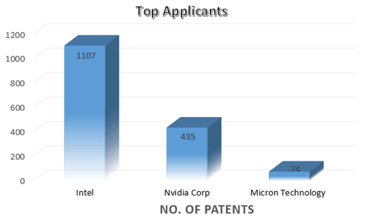
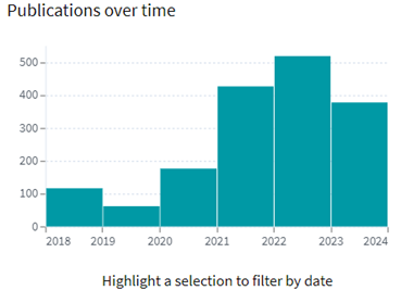

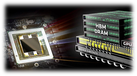
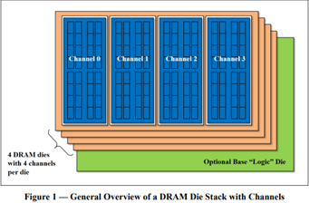
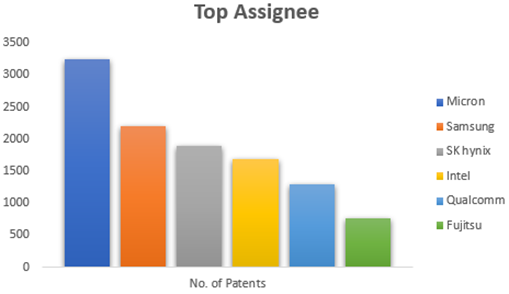
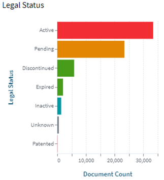
![High Bandwidth Memory 3 (HBM3): Overcoming Memory Bottlenecks in AI Accelerators With the rise of generative AI models that can produce original text, picture, video, and audio material, artificial intelligence (AI) has made major strides in recent years. These models, like large language models (LLMs), were trained on enormous quantities of data and need a lot of processing power to function properly. However, because of their high cost and processing requirements, AI accelerators now require more effective memory solutions. High Bandwidth Memory, a memory standard that has various benefits over earlier memory technologies, is one such approach. How HBM is relevant to AI accelerators? Constant memory constraints have grown problematic in a number of fields over the past few decades, including embedded technology, artificial intelligence, and the quick growth of generative AI. Since external memory interfaces have such a high demand for bandwidth, several programs have had trouble keeping up. An ASIC (application-specific integrated circuit) often connects with external memory, frequently DDR memory, through a printed circuit board with constrained interface capabilities. The interface with four channels only offers about 60 MB/s of bandwidth even with DDR4 memory. While DDR5 memory has improved in this area, the improvement in bandwidth is still just marginal and cannot keep up with the continuously expanding application needs. However, a shorter link, more channels, and higher memory bandwidth become practical when we take the possibility of high memory bandwidth solutions into account. This makes it possible to have more stacks on each PCB, which would greatly enhance bandwidth. Significant advancements in high memory bandwidth have been made to suit the demands of many applications, notably those demanding complex AI and machine learning models. Latest generation of High Bandwidth Memory The most recent high bandwidth memory standard is HBM3, which is a memory specification for 3D stacked SDRAM that was made available by JEDEC in January 2022. With support for greater densities, faster operation, more banks, enhanced reliability, availability, and serviceability (RAS) features, a lower power interface, and a redesigned clocking architecture, it provides substantial advancements over the previous HBM2E standard (JESD235D). [Source: HBM3 Standard [JEDEC JESD238A] Page 16 of 270] P.S. You can refer to HBM3 Standard [JEDEC JESD238A]: https://www.jedec.org/sites/default/files/docs/JESD238A.pdf for further studies. How does HBM3 address memory bottlenecks in AI accelerators? HBM3 is intended to offer great bandwidth while consuming little energy, making it perfect for AI tasks that need quick and effective data access. HBM3 has a number of significant enhancements over earlier memory standards, including: Increased bandwidth Since HBM3 has a substantially larger bandwidth than its forerunners, data may be sent between the memory and the GPU or CPU more quickly. For AI tasks that require processing massive volumes of data in real-time, this additional bandwidth is essential. Lower power consumption Since HBM3 is intended to be more power-efficient than earlier memory technologies, it will enable AI accelerators to use less energy overall. This is crucial because it may result in considerable cost savings and environmental advantages for data centers that host large-scale AI hardware. Higher memory capacity Greater memory capacities supported by HBM3 enable AI accelerators to store and analyze more data concurrently. This is crucial for difficult AI jobs that need access to a lot of data, such as computer vision or natural language processing. Improved thermal performance AI accelerators are less likely to overheat because to elements in the architecture of HBM3 that aid in heat dissipation. Particularly during demanding AI workloads, this is essential for preserving the system's performance and dependability. Compatibility with existing systems Manufacturers of AI accelerators will find it simpler to implement the new technology because HBM3 is designed to be backward-compatible with earlier HBM iterations without making substantial changes to their current systems. This guarantees an easy switch to HBM3 and makes it possible for quicker integration into the AI ecosystem. In a word, HBM3 offers enhanced bandwidth, reduced power consumption, better memory capacity, improved thermal performance, and compatibility with current systems, making it a suitable memory choice for AI accelerators. HBM3 will play a significant role in overcoming memory constraints and allowing more effective and potent AI systems as AI workloads continue to increase in complexity and size. Intellectual property trends for HBM3 in AI Accelerators HBM3 in AI Accelerators is witnessing rapid growth in patent filing trends across the globe. Over the past few years, the number of patent applications almost getting doubled every two years. MICRON is a dominant player in the market with 50% patents. It now holds twice as many patents as Samsung and SK Hynix combined. Performance, capacity, and power efficiency in today's AI data centers are three areas where Micron's HBM3 Gen2 "breaks new records." It is obvious that the goal is to enable faster infrastructure utilization for AI inference, lower training periods for big language models like GPT-4, and better total cost of ownership (TCO). Other key players who have filed for patents in High bandwidth memory technology with are Intel, Qualcomm, Fujitsu etc. [Source: https://www.lens.org/lens/search/patent/list?q=stacked%20memory%20%2B%20artificial%20intelligence] Following are the trends of publication and their legal status over time: [Source: https://www.lens.org/lens/search/patent/list?q=stacked%20memory%20%2B%20artificial%20intelligence] These Top companies own around 60% of total patents related to UFS. The below diagram shows these companies have built strong IPMoats in US jurisdiction. [Source: https://www.lens.org/lens/search/patent/list?q=stacked%20memory%20%2B%20artificial%20intelligence] Conclusion In summary, compared to earlier memory standards, HBM3 provides larger storage capacity, better bandwidth, reduced power consumption, and improved signal integrity. HBM3 is essential for overcoming memory limitations in the context of AI accelerators and allowing more effective and high-performance AI applications. HBM3 will probably become a typical component in the next AI accelerator designs as the need for AI and ML continues to rise, spurring even more improvements in AI technology. Meta Data The performance of AI accelerators will be improved by the cutting-edge memory technology HBM3, which provides unparalleled data speed and efficiency.](https://intellect-partners.com/wp-content/uploads/2023/12/Blog-Cover-2.png)