Categories
Computer Science

Demystifying Kubernetes: A Comprehensive Guide to Container Orchestration

What is Kubernetes?

Kubernetes (K8s) is an open-source platform that facilitates the execution of containerized applications in a virtual environment via Application Program Interfaces (APIs). Containerized applications are programs that are executed in containers. Containers are the virtual entities that hold the primary code for the execution of an application, its dependencies of that application and the configuration files of that application. Containerized applications are widely adapted because they facilitate the execution of multiple applications in a single host by isolating them from the core Operating System. This makes Kubernetes a go-to for users/developers to test, assess, and deploy their applications.

Kubernetes Architecture

Kubernetes employs a Master-Slave architecture. Kubernetes Cluster is divided into two separate planes:

i. Control Plane: Also known as the Master Node, the Control plane can be interpreted as the brains of Kubernetes. It is the policy maker that applications executed in Kubernetes clusters have to follow. It consists of:

a. API server: The API server is the entity that authenticates and authorizes a developer and allows interaction between the developer and Kubernetes Cluster. The API server configures and manipulates entities in the data plane via Kubernetes Controller-Manager, Kubernetes Scheduler, and Key-Value Store (Etcd).
b. Kubernetes Controller-Manager: It is the entity in the Control Plane that is responsible for keeping the system in a desired state, as per the instructions obtained from the API server. It constantly monitors the containers, Pods, and Nodes and tweaks them to bring them to the desired state.
c. Kubernetes Scheduler: It is the entity in the Control plane responsible for deploying applications in Worker Nodes received through the API server. It schedules the applications as per their requirements of resources, like memory, identifies suitable Pods, and places them in suitable Worker Nodes in the Kubernetes Clusters.
d. Key-Value Store (Etcd): It is a storage that can be placed within the control plane or independent of it. Key-value Store, as the name suggests, stores all the data of the Kubernetes Cluster, i.e., it provides a restore point to the whole of the Kubernetes Cluster.

ii. Data Plane: The Data Plane is a cluster of Kubernetes Worker Nodes that executes the policies made by the Control plane for the smooth operation of applications within the Kubernetes Cluster. Worker nodes are the machines that run containerized applications and provide the necessary resources for the applications to run smoothly. Each Worker Node consists of:
a. Kubelet: Kubelet is the entity within the Worker Node that is responsible for connecting that node with the API server in the Control Plane and reporting the status of Pods and containers within the node. This facilitates the resources assigned to that node to become a part of the Kubernetes Cluster. It is also responsible for the execution of works received from the API server to keep the node in a desired state by making the necessary changes as per API server instructions.
b. Kube-proxy: It is responsible for routing traffic from the users through the Internet to the correct applications within a node by creating/altering traffic routing policies for that node.
c. Pods:  Pods are the entities in the Worker Node that have containers within them. Although it is possible to host multiple application instances in a Pod, running one application instance in one Pod is recommended. Pods are capable of horizontal scaling, i.e., they are created according to the application instance needs. If assigned node resources are available, Pods can utilize more resources than assigned to them- if needed. Pods, along with containers, are capable of running on multiple machines. The resources of the Pods are shared among the containers it hosts.

HBM Layout: Deploying an Application in Kubernetes

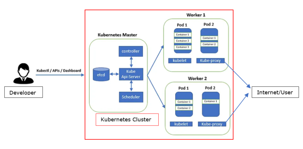
HBM Layout (Source: Medium)

Deploying an Application in Kubernetes:

i. The developer should have a Service account. This account is needed to authenticate and authorize a developer. Also, this service account is used for authentication against the API server when the application needs access to protected resources.

Kubernetes Service Account Requirement

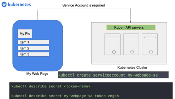
Service Account Requirement (Source: Medium)

ii. Create a new Node or select an existing node according to the application requirement (memory, RAM, etc).

iii. The intended application should be packed in a Docker image or similar container format. A Docker image is a software package that has all the necessary programs, dependencies, runtimes, libraries, and configuration files for an application to run smoothly.

iv. The developer should define Kubernetes Manifest as a YAML or JASON file. The Kubernetes Manifest defines the desired state for the application to be deployed. It consists of:
a. Configmaps: As the name suggests, Configmaps have configuration data of the application to be deployed. It has supporting configurations, like environment variables for the intended application. The total size of this data is less than 1MB.
b. Secrets: Kubernetes secrets are similar to Configmaps, but hold secure information. They hold supporting files, like passwords, for the application that is to be deployed.
c. Deployments: Deployments define the procedure of creating and updating application instances for the application to be deployed.
d. Kubernetes Service: It is the entity that assigns an IP address or hostname to the application that is to be deployed. When the assigned name is matched to a user’s search string, the application is presented to the user through the internet via Kube Proxy.

v. The developer places the Docker image through the Kubernetes API server. The API server pulls the Docker image to create the containers in the Pods, to deploy the intended application.

vi. Once the intended application is deployed in the pods, the developer can monitor, update, change, and edit the application as per the requirement through Kubectl from the developers’ service account through the API server in the control panel.

Kubernetes Deployment Flow

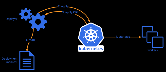
Deployment Flow (Source: Polarsquad)

Categories
Electronics

From Wallets to UPI: Transforming the Payments Landscape

Unified Payments Interface

The Unified Payments Interface (UPI) has become a revolutionary force in the fast-paced and constantly changing field of financial technology, completely changing the way digital transactions are conducted in India. UPI, which was created by the National Payments Corporation of India (NPCI), is evidence of the nation’s dedication to promoting an equitable digital economy. Through an examination of UPI’s history, quick uptake, and significant influence on how people and companies handle their financial transactions, this introduction aims to shed light on the relevance of the technology. Officially introduced in April 2016, UPI was born out of the demand for a more convenient and interoperable payment mechanism. UPI was the idea of NPCI, a project supported by major banks and the Reserve Bank of India with the goal of streamlining the difficulties involved in conventional banking procedures.

The goal was very clear: to develop a platform that would enable consumers to use their phones to complete safe, quick, and seamless transactions. UPI has seen an unheard-of rise in popularity since its launch, completely changing how individuals send and receive money as well as how they pay for goods and services. With its easy-to-use interface and ability to conduct transactions without requiring lengthy bank data, UPI has become the leading digital payment option. Because of its straightforward design and the widespread use of smartphones, financial transactions have become more accessible to people from a wider range of socioeconomic backgrounds. A network of banks, financial institutions, and third-party service providers that have adopted this cutting-edge technology define the UPI ecosystem. The user experience has been further streamlined with the advent of Virtual Payment Addresses (VPAs), which enable transactions utilizing unique IDs rather than conventional bank account information.

In July 2022, over 200 million UPI transactions were made every day

HBM Layout (Source: NPCI)

In the current digital age, where ease and speed are critical, UPI has come to represent financial emancipation. Because of its real-time settlement, bank-to-bank interoperability, and ongoing innovation from different service providers, UPI is now considered a pillar of India’s digital financial infrastructure. It is clear as we dig deeper into the details of UPI—from its benefits and drawbacks to the inner workings of the market and backend—that it is more than just a payment interface. Rather, it is a driving force behind a significant change in the way financial transactions are carried out, ushering in a new era in India’s digital economy.

How UPI Works

NPCI’s Role: The National Payments Corporation of India (NPCI) plays a pivotal role in the backend operations of UPI. It operates the central switch that facilitates the routing of transactions between different banks. Acting as an umbrella organization for retail payments, NPCI ensures interoperability among various banks and service providers.

UPI Servers and Infrastructure: The backbone of UPI is a robust server infrastructure that manages the vast volume of transactions in real-time. UPI servers act as the intermediaries that process and route transaction requests between the sender’s and recipient’s banks.

Bank Servers and Integration: Each participating bank in the UPI ecosystem maintains its servers that are integrated with the UPI platform. These servers are responsible for handling transaction requests from their respective customers. The integration ensures that the UPI system can communicate seamlessly with the individual banking systems.

Unique IDs and Virtual Payment Addresses (VPAs): At the heart of UPI transactions are the unique identifiers known as Virtual Payment Addresses (VPAs). These VPAs, in the form of “yourname@bank,” serve as the user’s identity and eliminate the need for sharing sensitive information like account numbers and IFSC codes during transactions.

APIs and Protocols: Application Programming Interfaces (APIs) are the bridges that enable communication between different entities in the UPI ecosystem. UPI relies on standardized protocols and APIs to ensure that transactions are executed smoothly across various banks and UPI-enabled apps.

Transaction Request Flow: When a user initiates a UPI transaction, the request flows through a predefined sequence of steps. The sender’s UPI app sends a request to the UPI server, specifying the recipient’s VPA and the transaction amount. The UPI server then communicates with the sender and recipient banks to verify and authorize the transaction.

Authentication Mechanism: Security is a top priority in UPI transactions. The backend employs strong authentication mechanisms, typically involving a secure Personal Identification Number (PIN). This PIN ensures that only the authorized user can initiate and approve transactions.

Real-Time Settlement: UPI is known for its real-time settlement feature. Once the transaction is authenticated, the backend systems ensure an immediate transfer of funds from the sender’s bank to the recipient’s bank. This quick settlement is a key factor in the widespread adoption and popularity of UPI.

Transaction Status and Confirmation: Throughout the process, the backend systems keep track of the transaction status. Both the sender and the recipient receive immediate notifications and confirmations, providing transparency and assurance about the success of the transaction.

Continuous Monitoring and Security Measures: The backend operations of UPI involve continuous monitoring for any suspicious activities or potential security threats. Robust security measures, including encryption and multi-factor authentication, are in place to safeguard user data and financial transactions.

UPI Transactions Backend

UPI working (Source: Payu)

Advantages of UPI

Seamless Transactions: UPI facilitates seamless transactions by eliminating the need for traditional banking processes. Users can send and receive money with just a few taps on their smartphones, making it incredibly user-friendly.

24/7 Accessibility: Unlike traditional banking hours, UPI transactions can be conducted 24/7, providing users with unparalleled accessibility and flexibility. This round-the-clock availability has significantly enhanced the efficiency of financial transactions.

Interoperability: UPI is designed to be interoperable across various banks, allowing users to link multiple bank accounts to a single UPI ID. This interoperability promotes financial inclusivity and ensures that users are not restricted to a particular banking network.

Instant Fund Transfer: One of the key advantages of UPI is its real-time fund transfer capability. Money is transferred instantly between accounts, reducing the waiting time associated with traditional banking methods like NEFT or RTGS.

QR Code Integration: UPI payments are further simplified through the integration of QR codes. Users can scan QR codes to initiate transactions, making it a convenient option for both merchants and consumers.

Disadvantages of UPI

Cybersecurity Concerns: With the surge in digital transactions, UPIs have become a target for cybercriminals. Issues such as phishing attacks and fraudulent transactions pose significant challenges, emphasizing the need for robust cybersecurity measures.

Dependency on Technology: UPI transactions heavily depend on technology and internet connectivity. This dependency may pose challenges for users in remote areas with limited access to a stable internet connection.

Transaction Limits: While UPI supports quick transactions, there are often limits imposed on the amount that can be transferred in a single transaction. This limitation can be inconvenient for users looking to make large transactions.

Lack of Awareness: Despite its widespread adoption, there is still a segment of the population unfamiliar with UPI. The lack of awareness and understanding of digital payment systems may hinder its full-scale adoption across all demographics.

Market Players and Competition

PhonePe: PhonePe, a popular UPI-based payment app, has gained significant traction with its user-friendly interface and seamless integration with various services. Acquired by Flipkart, PhonePe has become a major player in the digital payment space.

Google Pay: Google Pay, powered by UPI, has emerged as a strong contender in the market. Its integration with the Android ecosystem and intuitive features has attracted a large user base, making it a dominant force in the UPI landscape.

Paytm: Paytm, initially known for its mobile wallet, has seamlessly integrated UPI into its platform. With a diverse range of services, including bill payments and online shopping, Paytm remains a prominent player in the UPI market.

BHIM (Bharat Interface for Money): Developed by NPCI, BHIM is a UPI-based app that aims to simplify digital transactions for users across different banks. Its focus on promoting financial inclusion and interoperability makes it a notable player in the UPI space.

Categories
Electronics Others

Migration from Hybrid Memory Cube (HMC) to High-Bandwidth Memory (HBM)

Introduction:

Memory technology plays a vital role in providing effective data processing as the demand for high-performance computing keeps rising. The industry has recently seen a considerable migration from Hybrid Memory Cube (HMC) to High-Bandwidth Memory (HBM) because of HMB’s higher performance, durability, and scalability. This technical note talks about the causes behind the widespread adoption of HBM as well as the benefits it has over HMC.

HBM Overview:

HBM is a revolutionary memory technology that outperforms conventional memory technologies. HBM is a vertically stacked DRAM memory device interconnected to each other using through-silicon vias (TSVs). HBM DRAM die is further tightly connected to the host device using its distribution channels which are completely independent of one another. This architecture is used to achieve high-speed, low-power operation. HBM has a reduced form factor because it combines DRAM dies and logic dies in a single package, making it ideal for space-constrained applications. An interposer that is interconnected to the memory stacks, enables high-speed data transmission between memory and processor units. 

HMC Brief:

The Hybrid Memory Cube (HMC) comprises multiple stacked DRAM dies and a logic die, stacked together using through-silicon via (TSV) technology in a single-package 3D-stacked memory device. The HMC stack’s memory dies each include their memory banks as well as a logic die for memory access control. It was developed by Micron Technology and Samsung Electronics Co. Ltd. in 2011, and announced by Micron in September 2011.

When compared to traditional memory architectures such as DDR3, it enables faster data access and lower power consumption. Each memory in HMC is organized into a vault. Each vault in the logic die has a memory controller which manages memory operations. HMC is used in applications where speed, bandwidth, and sizes are more required. Micron discontinued the use of HMC in 2018 when it failed to become successful in the semiconductor industry.

Hybrid Memory Cube (HMC) and High-Bandwidth Memory (HBM) are two distinct memory technologies that have made significant contributions to high-performance computing. While both of these technologies aim to enhance memory bandwidth operation, there are many fundamental distinctions between HMC and HBM.

Power Consumption: HBM significantly has lower power consumption compared to HMC. HBM’s vertical stacking approach eliminates high-power consumption bus interfaces and reduces the distance for data transfer between DRAM dies, resulting in improved energy efficiency. This decreased power usage is especially beneficial in power-constrained environments like mobile devices or energy-efficient servers.

Memory Architecture: HMC uses a 3D-stacked memory device comprised of several DRAM dies and a logic die stacked together via through-silicon (TSV) technology. In addition to its memory banks, each memory die in the HMC stack contains a logic die for a memory access operation. HBM, on the other hand, is a 3D-stacked architecture that integrates base (logic) die and memory dies as well as a processor (GPU) on a single package that is coupled by TSVs to provide a tightly coupled high-speed processing unit. The memory management process is made easier by the shared memory space shared by the memory dies in an HBM stack.

Industry Adoption: When compared to HMC, HBM offers more memory density in a smaller physical footprint. HBM does this by vertically stacking memory dies on a single chip, resulting in increased memory capacity in a smaller form factor. HBM is well-suited for space-constrained applications such as graphics cards and mobile devices because of its density.

Memory Density: In comparison to HMC, HBM frequently utilizes less energy and power. The vertical stacking strategy used by HBM shortens the transfer of data distance and removes power-hungry bus connections, resulting in increased energy efficiency. This decreased power usage is especially beneficial in power-constrained contexts like mobile devices or energy-efficient servers.

Memory Bandwidth: Comparing HMC and HBM to conventional memory technologies, they both offer much better memory bandwidth. On the other hand, HBM often delivers higher bandwidth compared to HMC. By using a wider data channel and higher signaling rates, HBM accomplishes this, enabling faster data flow between the processor and the memory units.

In conclusion, HMC and HBM differ in terms of memory bandwidth, architecture, power consumption, density, and industry recognition. While HMC offers significantly better performance over conventional memory technologies, HBM has become the market leader due to its reduced form factor, higher performance, and efficiency, which has expedited the transition from HMC to HBM.

Advantages of HBM:

Power Consumption: HBM uses less energy and power for data transfer on the I/O interface than HMC, hence lowering energy efficiency. HBM improves energy efficiency by using vertical stacking technology to reduce data transfer distance and power-intensive bus interfaces.

Bandwidth: HBM provides excellent memory bandwidth, allowing the processor/controller to quickly access data to obtain greater speed. HBM has more memory channels and along with high-speed signaling than HMC, which allows for more bandwidth. This high bandwidth is critical for data-intensive applications such as AI, machine learning, and graphics.

Scalability: By enabling the connection of different memory stacks, HBM offers scalable memory configurations. Because of this flexibility, numerous memory and bandwidth options are available to meet the unique needs of various applications.

Density: With a reduced size, HBM’s vertical stacking technique makes greater memory densities possible. HBM memory is ideal for smaller devices such as mobile phones and graphics cards etc. Enhanced system performance is also made possible by higher memory density by lowering data access latency.

Signal Integrity: TSV-based interconnects in HBM provide superior signal integrity than wire-bonded techniques. The reduced data transmission failures and increased system dependability are both benefits of improved signal integrity.

Conclusion:

A significant development in memory technology is the change from HMC to HBM. The requirement for faster and more effective memory solutions has been spurred by the demand for high-performance computing, particularly in fields like AI, machine learning, and graphics. With its different benefits, HBM is broadly utilized in various ventures because of its high bandwidth, low power consumption, increased density, versatility, and improved signal integrity. HBM has become the standard option for high-performance memory needs, and its continuous development is expected to influence the direction of memory technologies in the market.