San Francisco-based intellectual property startup Fearn has announced the completion of a $5.5 million seed funding round to expand its AI-native patent drafting platform.
The round was led by Kindred Ventures, with participation from Andreessen Horowitz’s a16z speedrun startup accelerator, Designer Fund, and Essence VC. Prior to this institutional round, the company operated via founder self-funding.
The Founders and the Logic of Automation
Fearn was founded in 2025 by CEO Han Kim and CTO Angela Gao, who met as graduate students at Caltech. The platform’s architectural focus stems directly from the co-founders’ specialized backgrounds:
- Han Kim: Previously prosecuted patent applications across software, life sciences, and mechanical arts as a scientific analyst at Morrison & Foerster, while researching bio-inspired neural algorithms during his Ph.D. track at Caltech.
- Angela Gao: Completed a Ph.D. in computing and mathematical sciences at Caltech, specializing in physics-aligned generative models, alongside previous model development work at Google Research.
Kim noted that his experience in Big Law highlighted systemic inefficiencies in the traditional patent pipeline, which is frequently slow, cost-prohibitive, and anxiety-inducing for engineers worried about technical details being misinterpreted.
“I noticed a lot of the tasks I was doing could be automatable, but obviously I couldn’t automate them. You’re not really allowed to in those sorts of settings and environments,” Kim stated, highlighting the strict procedural friction within traditional law firms that inspired him to build an external automation solution.
How the Multi-Model Stack Works
Unlike general-purpose generative AI tools or simple API wrappers, Fearn is built from the ground up as a fully data-sovereign, AI-native platform. The coordinates a specialized multi-model stack:
- Bespoke Model Ensemble: The platform utilizes dozens of hypercompact, specialized models, combining proprietary code, fine-tuned open-source models, and symbolic non-LLM systems built from scratch.
- Data Sovereignty: Fearn hosts 100% of its own model stack internally. It makes zero application programming interface (API) calls to third-party model developers, completely removing the public-disclosure and data-egress risks that typically restrict enterprise IP teams from leveraging generative AI.
- Hallucination Resistance: By training its custom architectures on highly curated, hand-corrected, and hand-labeled intellectual property datasets, Fearn creates audit trails engineered to guarantee compliance with patent office requirements and eliminate the factual errors common in large language models.
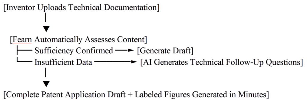
Once the application and automated labeled figures are ready, corporate research teams or solo inventors can choose to file the paperwork independently or hand it off to external counsel for final strategic review. Fearn charges a flat, predictable fee of $2,000 per patent draft, cutting traditional preparation timelines down significantly.
Future Plans and the Legal Tech Boom
With a lean team of fewer than 10 people, Fearn plans to deploy the capital injection primarily toward technical hiring, infrastructure expansion, and offsetting computational overhead.
Looking forward, the company intends to scale its features to assist inventors throughout the entire end-to-end patent prosecution lifestyle. This includes expanding automated systems to handle office action responses and any procedural workflow tied directly to a U.S. Patent and Trademark Office (USPTO) registration number.
Fearn’s successful seed round emphasizes an accelerating streak of legal tech investments by Andreessen Horowitz. The firm’s recent IP and legal portfolio expansion includes:
- Leading patent automation startup Stilta’s seed round.
- Anchoring multiple massive funding rounds for legal AI platform Harvey.
- Backing litigation-focused developer Eve across two distinct rounds.
- Leading the pre-seed round for communication security provider ZeroDrift.